# RAA489400 Datasheet
## 2. Pin Information
### 2.1 Pin Assignments
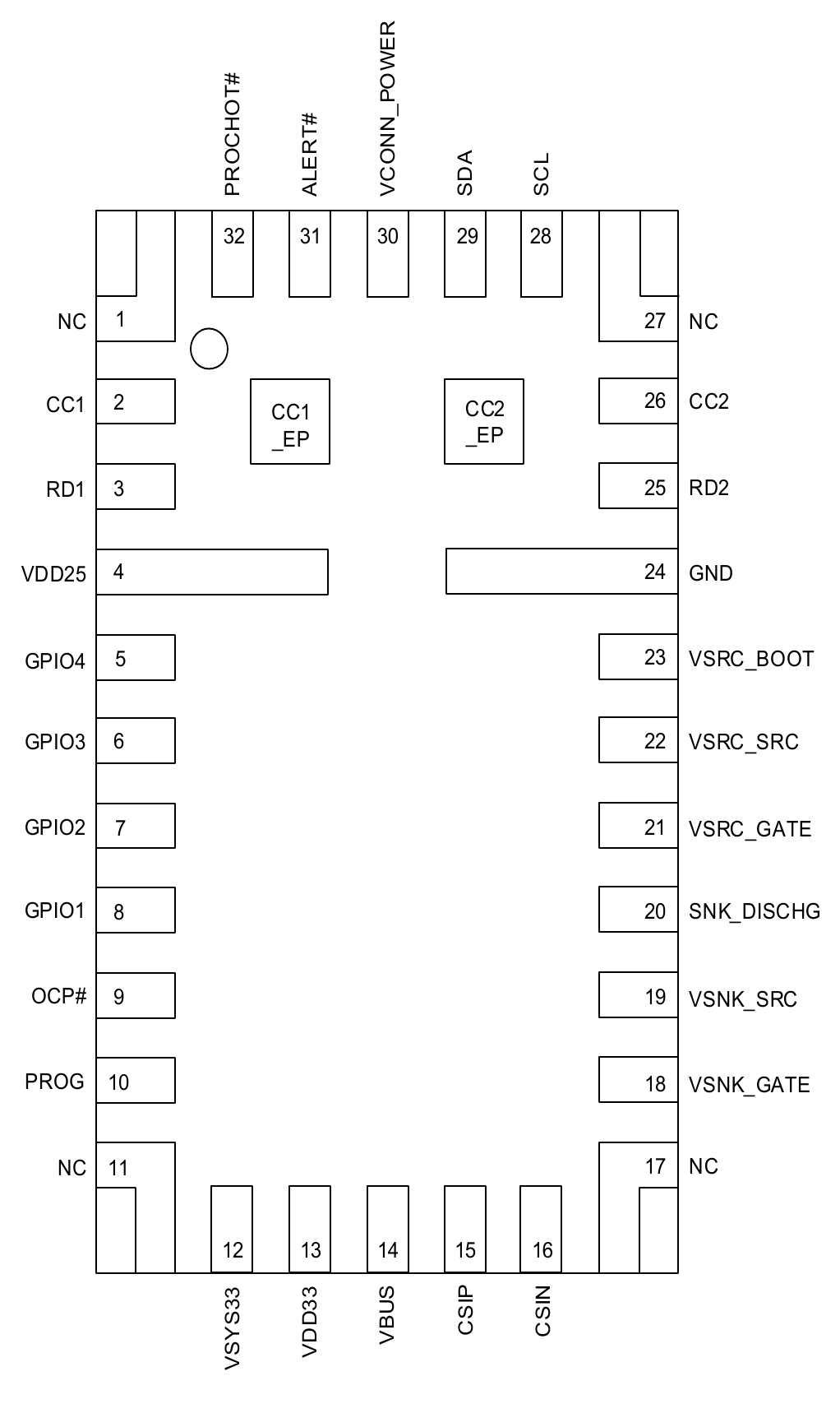
Pin numbers and names read from the drawing:
| Side | Pin Number | Pin Name |
|---|---|---|
| Left | 1 | `NC` |
| Left | 2 | `CC1` |
| Left | 3 | `RD1` |
| Left | 4 | `VDD25` |
| Left | 5 | `GPIO4` |
| Left | 6 | `GPIO3` |
| Left | 7 | `GPIO2` |
| Left | 8 | `GPIO1` |
| Left | 9 | `OCP#` |
| Left | 10 | `PROG` |
| Left | 11 | `NC` |
| Bottom | 12 | `VSYS33` |
| Bottom | 13 | `VDD33` |
| Bottom | 14 | `VBUS` |
| Bottom | 15 | `CSIP` |
| Bottom | 16 | `CSIN` |
| Right | 17 | `NC` |
| Right | 18 | `VSNK_GATE` |
| Right | 19 | `VSNK_SRC` |
| Right | 20 | `SNK_DISCHG` |
| Right | 21 | `VSRC_GATE` |
| Right | 22 | `VSRC_SRC` |
| Right | 23 | `VSRC_BOOT` |
| Right | 24 | `GND` |
| Right | 25 | `RD2` |
| Right | 26 | `CC2` |
| Right | 27 | `NC` |
| Top | 28 | `SCL` |
| Top | 29 | `SDA` |
| Top | 30 | `VCONN_POWER` |
| Top | 31 | `ALERT#` |
| Top | 32 | `PROCHOT#` |
| Exposed pad | `CC1_EP` | `CC1` exposed pad |
| Exposed pad | `CC2_EP` | `CC2` exposed pad |
### 2.2 Pin Descriptions
| Pin Number | Pin Name | Description |
|---|---|---|
| 1 | `NC` | No connection |
| 2 | `CC1` | Configuration Channel 1, Analog pin from CC-PHY. |
| 3 | `RD1` | Dead battery Rd, Analog pin from CC-PHY. Tie to `CC1` when dead battery Rd is supported. |
| 4 | `VDD25` | 2.5V LDO output provides the bias power for internal digital logic and the TCPC transmitter. Connect a ceramic capacitor to GND. The effective capacitance of `VDD25` capacitor should be at least 1µF at 2.5V. This pin cannot source current to external circuits. |
| 5 | `GPIO4` | General purpose input and output with a 3.3V push-pull output, 1.8V or 3.3V open-drain output, 1.8V or 3.3V input, or disable. It can be used as a VBUS source or a sink switch control and overcurrent input.
• VBUS source power switch enable
• VBUS sink power switch enable
• Overcurrent Input (from external VBUS source power switch)
• General Purpose Input
• General Purpose Output (push-pull)
• General Purpose Output (open-drain)
`GPIO1_CTRL` Register, `GPIO2_CTRL` Register, `GPIO3_CTRL` Register, `GPIO4_CTRL` Register, `VBUS_PATH_CTRL` Register, `VBUS_GPIO_CTRL` Register, and `GPIO_OC_EN` Register control those configurations. |
| 6 | `GPIO3` | General purpose input and output with a 3.3V push-pull output, 1.8V or 3.3V open-drain output, 1.8V or 3.3V input, or disable. It can be used as a VBUS source or a sink switch control and overcurrent input.
• VBUS source power switch enable
• VBUS sink power switch enable
• Overcurrent Input (from external VBUS source power switch)
• General Purpose Input
• General Purpose Output (push-pull)
• General Purpose Output (open-drain)
`GPIO1_CTRL` Register, `GPIO2_CTRL` Register, `GPIO3_CTRL` Register, `GPIO4_CTRL` Register, `VBUS_PATH_CTRL` Register, `VBUS_GPIO_CTRL` Register, and `GPIO_OC_EN` Register control those configurations. |
| 7 | `GPIO2` | General purpose input and output with a 3.3V push-pull output, 1.8V or 3.3V open-drain output, 1.8V or 3.3V input, or disable. It can be used as a VBUS source or a sink switch control and overcurrent input.
• VBUS source power switch enable
• VBUS sink power switch enable
• Overcurrent Input (from external VBUS source power switch)
• General Purpose Input
• General Purpose Output (push-pull)
• General Purpose Output (open-drain)
`GPIO1_CTRL` Register, `GPIO2_CTRL` Register, `GPIO3_CTRL` Register, `GPIO4_CTRL` Register, `VBUS_PATH_CTRL` Register, `VBUS_GPIO_CTRL` Register, and `GPIO_OC_EN` Register control those configurations. |
| 8 | `GPIO1` | General purpose input and output with a 3.3V push-pull output, 1.8V or 3.3V open-drain output, 1.8V or 3.3V input, or disable. It can be used as a VBUS source or a sink switch control and overcurrent input.
• VBUS source power switch enable
• VBUS sink power switch enable
• Overcurrent Input (from external VBUS source power switch)
• General Purpose Input
• General Purpose Output (push-pull)
• General Purpose Output (open-drain)
`GPIO1_CTRL` Register, `GPIO2_CTRL` Register, `GPIO3_CTRL` Register, `GPIO4_CTRL` Register, `VBUS_PATH_CTRL` Register, `VBUS_GPIO_CTRL` Register, and `GPIO_OC_EN` Register control those configurations. |
| 9 | `OCP#` | Open-drain output with 1.8V or 3.3V pull-up.
Active low when a fault condition configured in `OCP_OUTPUT_CTRL` Register (A8h) is detected.
When all fault conditions are removed, `OCP#` pin is deasserted to high. |
| 10 | `PROG` | A resistor from the `PROG` pin to GND to set the SMBus/I²C slave target address. |
| 11 | `NC` | No connection |
| 12 | `VSYS33` | Main power input (minimum 3.0V, typical 3.3V). Connect a ceramic capacitor to GND. Recommended capacitance: 4.7µF. |
| 13 | `VDD33` | 3.3V LDO output provides the bias power for the internal analog and digital circuit. It also supplies power for the external TCPM.
Connect a ceramic capacitor to GND. The effective capacitance of `VDD33` capacitor should be at least 1µF at 3.3V.
Do not apply additional load on the `VDD33` pin other than TCPM and a pull-up resistor for `SDA`/`SCL`/`ALERT#` between RAA489400 and TCPM.
*Note:* If two or more RAA489400 `VDD33` supplies 3.3V to TCPM, a diode is required for each `VDD33` pin. |
| 14 | `VBUS` | VBUS voltage sense and discharge input.
Input for internal LDO power on dead battery mode (`VSYS33` = 0V). |
| 15 | `CSIP` | Connect to the VBUS source current-sense resistor positive input through a resistor. Place a ceramic capacitor between `CSIP` and `CSIN` to provide differential-mode filtering.
The current sense resistor value must be 10mΩ. |
| 16 | `CSIN` | Input for sensing VBUS voltage. Connect to the VBUS source current-sense resistor negative input. Use a Kelvin line between the voltage sense point and `CSIN`. |
| 17 | `NC` | No connection |
| 18 | `VSNK_GATE` | Gate drive output of N-channel MOSFET USB-C/PD VBUS sink path FET. |
| 19 | `VSNK_SRC` | N-channel MOSFET source input reference for USB-C/PD VBUS sink path FET(s). |
| 20 | `SNK_DISCHG` | Internal system sink path discharge between the VBUS sink path gate and system load (such as battery charger adapter side). |
| 21 | `VSRC_GATE` | Gate drive output of N-channel MOSFET USB-C/PD Source FET, pumped 5V above `VSRC_SRC`. |
| 22 | `VSRC_SRC` | N-channel MOSFET source input reference for USB-C/PD VBUS Source path FET(s). |
| 23 | `VSRC_BOOT` | Connect external capacitor for charge pump of `VSRC_GATE`.
Recommended capacitance: 0.047µF. |
| 24 | `GND` | Ground |
| 25 | `RD2` | Dead battery Rd, Analog pin from CC-PHY. Tie to `CC2` when dead battery Rd is supported. |
| 26 | `CC2` | Configuration Channel 2, Analog pin from CC-PHY. |
| 27 | `N.C.` | No connection |
| 28 | `SCL` | SMBus/I²C clock I/O. Connect to the clock line from TCPM for TCPC control. |
| 29 | `SDA` | SMBus/I²C data I/O. Connect to the data line from TCPM for TCPC control. |
| 30 | `VCONN_POWER` | 5V Input to the VCONN MUX providing power to the `CC1`/`CC2` and the `VSRC_GATE` driver.
Connect a ceramic capacitor to GND.
The `VCONN_POWER` capacitor should be at least 4.7µF. |
| 31 | `ALERT#` | Interrupt line for `SDA` and `SCL`. |
| 32 | `PROCHOT#` | Open-drain output with 1.8V or 3.3V pull-up.
Active low when either VBUS source device disconnection or Sink Fast Role Swap is detected. The assertion condition configured in `PROCHOT_EN` Register (AAh) is detected.
When the condition is removed, the `PROCHOT#` pin is deasseted to high. |
| `CC1-EP` | `CC1` | Exposed pad for `CC1`. |
| `CC2-EP` | `CC2` | Exposed pad for `CC2`. |
### 2.3 Unused Pin Termination
| Pin Number | Pin Name | Connection Method |
|---|---|---|
| 1, 11, 17, 27 | `NC` | Open |
| 3 | `RD1` | Open |
| 5 | `GPIO4` | Open |
| 6 | `GPIO3` | Open |
| 7 | `GPIO2` | Open |
| 8 | `GPIO1` | Open |
| 9 | `OCP#` | Open |
| 12 | `VSYS33` | Connect to GND if `VSYS33` is not used for start-up. |
| 18 | `VSNK_GATE` | Open |
| 19 | `VSNK_SRC` | Connect to GND through a 0Ω resistor. |
| 21 | `VSRC_GATE` | Open |
| 22 | `VSRC_SRC` | Connect to GND through a 0Ω resistor. |
| 23 | `VSRC_BOOT` | Open |
| 25 | `RD2` | Open |
| 30 | `VCONN_POWER` | Connect to `VDD33` if VCONN function is not used. |
| 32 | `PROCHOT#` | Open |
Notes:
1. In the original document, the description cell for pins 5–8 (`GPIO4`, `GPIO3`, `GPIO2`, `GPIO1`) is a single merged cell spanning all four rows; the text has been repeated for each pin row here.
2. In the original document, the connection method cell for pins 5–8 (`GPIO4`, `GPIO3`, `GPIO2`, `GPIO1`) in the Unused Pin Termination table is a single merged cell containing "Open"; the value has been repeated for each pin row here.