30 KiB
3. Specifications
3.1 Absolute Maximum Ratings
Caution: Do not operate at or near the maximum ratings listed for extended periods of time. Exposure to such conditions can adversely impact product reliability and result in failures not covered by warranty.
| Parameter | Minimum | Maximum | Unit |
|---|---|---|---|
CSIP, CSIN, DCIN, ADP, ASGATE |
-0.3 | +36 | V |
DCIN - VDD |
-0.3 | +31 | V |
PHASE1 |
GND - 0.3 | +36 | V |
PHASE1 |
GND - 2 (<20ns) | +36 | V |
BOOT1, UGATE1 |
GND - 0.3 | VDDP+36 | V |
PHASE2 |
GND - 0.3 | 36 | V |
PHASE2 |
GND - 2 (<20ns) | 36 | V |
BOOT2, UGATE2 |
GND - 0.3 | VDDP+36 | V |
LGATE1, LGATE2 |
GND - 0.3 | +6.5 | V |
LGATE1, LGATE2 |
GND - 2 (<20ns) | +6.5 | V |
VBAT, VSYS, CSOP, CSON, BGATE |
-0.3 | +36 | V |
VDD, VDDP |
-0.3 | +6.5 | V |
COMP |
-0.3 | +6.5 | V |
AMON/BMON, PSYS |
-0.3 | +6.5 | V |
OTGEN, BATGONE |
-0.3 | +6.5 | V |
ACIN, PROCHOT#, OTGPG, ACOK |
-0.3 | +6.5 | V |
SCL, SDA |
-0.3 | +6.5 | V |
BOOT1 - PHASE1, BOOT2 - PHASE2 |
-0.3 | +6.5 | V |
CSIP - CSIN, CSOP - CSON |
-0.3 | +0.3 | V |
OTGPG, PROCHOT#, ACOK |
- | 2 | mA |
| Junction Temperature Range (TJ) | -10 | +125 | °C |
| Storage Temperature Range (TS) | -65 | +175 | °C |
| Human Body Model (Tested per JS-001-2023) | - | 2 | kV |
| Charged Device Model (Tested per JS-002-2022) | - | 750 | V |
| Latch-Up (Tested per JESD78E; Class 2, Level A) | - | 100 | mA |
3.2 Recommended Operating Conditions
| Parameter | Parameter | Minimum | Maximum | Unit |
|---|---|---|---|---|
| Ambient Temperature | RAA489118ARGNP | -10 | +100 | °C |
| Ambient Temperature | RAA489118A3GNP | -40 | +100 | °C |
| Junction Temperature | RAA489118ARGNP | -10 | +125 | °C |
| Junction Temperature | RAA489118A3GNP | -40 | +125 | °C |
| Adapter Voltage | +4 | +30 | V |
3.3 Thermal Specifications
| Parameter | Package | Symbol | Conditions | Typical Value | Unit |
|---|---|---|---|---|---|
| Thermal Resistance | 32 Ld TQFN Package | θJA[1] | Junction to ambient. | 38 | °C/W |
| Thermal Resistance | 32 Ld TQFN Package | θJC[2] | Junction to case. | 2.5 | °C/W |
- θJA is measured in free air with the component mounted on a high-effective thermal conductivity test board with direct attach features. See TB379.
- For θJC, the case temperature location is the center of the exposed metal pad on the package underside.
3.4 Electrical Specifications
Operating conditions: ADP = CSIP = CSIN = 5V and 28V, VSYS = VBAT = CSOP = CSON = 8V and 29.4, unless otherwise noted. Boldface limits apply across the junction temperature range, -40°C to +125°C unless otherwise specified.
| Parameter | Symbol | Test Conditions | Min[1] | Typ | Max[1] | Unit |
|---|---|---|---|---|---|---|
| UVLO/ACOK | ||||||
| VADP UVLO Rising | VADP_UVLO_r |
- | 3.05 | 3.4 | 3.7 | V |
| VADP UVLO Hysteresis[2] | VADP_UVLO_h |
- | - | 600 | - | mV |
| VBAT UVLO Rising | VBAT_UVLO_r |
- | 2.30 | 2.45 | 2.65 | V |
| VBAT UVLO Hysteresis | VBAT_UVLO_h |
- | - | 400 | - | mV |
| VBAT 4P5V Rising | VBAT_4P5_r |
- | 4.25 | 4.50 | 4.90 | V |
| VBAT 4P5V Hysteresis | VBAT_4P5_h |
- | - | 400 | - | mV |
| VDD 2P7 POR Falling, SMBus and BGATE/BMON Active Threshold | VDD_2P7_f |
- | 2.5 | 2.7 | 2.9 | V |
| VDD 2P7 POR Hysteresis[2] | VDD_2P7_h |
- | - | 150 | - | mV |
| VDD 3P8 POR Rising, Modulator and Gate Driver Active | VDD_3P8_r |
- | 3.6 | 3.8 | 3.9 | V |
| VDD 3P8 POR Hysteresis | VDD_3P8_h |
- | - | 140 | - | mV |
| ACIN Rising | ACIN_r |
- | 0.58 | 0.6 | 0.615 | V |
| ACIN Hysteresis | ACIN_h |
- | - | 50 | - | mV |
| Linear Regulator | ||||||
| VDD Output Voltage | VDD |
6V < VDCIN < 30V | 4.5 | 5.0 | 5.5 | V |
| VDD Dropout Voltage | VDD_dp |
<35mA, VDCIN = 4V | - | - | 200 | mV |
| VDD Overcurrent Threshold | VDD_OC |
ARGNP Junction Temperature: -10 to +125°C | 85 | 115 | 145 | mA |
| VDD Overcurrent Threshold | VDD_OC |
A3GNP Junction Temperature: -40 to +125°C | 85 | 115 | 155 | mA |
Operating conditions: ADP = CSIP = CSIN = 5V and 28V, VSYS = VBAT = CSOP = CSON = 8V and 29.4, unless otherwise noted. Boldface limits apply across the junction temperature range, -40°C to +125°C unless otherwise specified. (Cont.)
| Parameter | Symbol | Test Conditions | Min[1] | Typ | Max[1] | Unit |
|---|---|---|---|---|---|---|
| Battery Current | IBAT1 | Battery only, BGATE OFF, PSYS OFF, GPC OFF, BMON OFF, VBAT = 29.4V, DCIN current comes from battery, IBAT = IVBAT + ICSOP + ICSON + IDCIN + IVSYS | - | 24 | 50 | µA |
| Battery Current | IBAT2 | Battery only, BGATE ON, PSYS OFF, GPC OFF, BMON ON, VBAT = 29.4V, DCIN current comes from battery, IBAT = IVBAT + ICSOP + ICSON + IDCIN + IVSYS | - | 74 | - | µA |
| Battery Current | IBAT3 | Battery only, BGATE on, PSYS ON, BMON OFF, VBAT = 29.4V, DCIN current comes from battery, IBAT = IVBAT + ICSOP + ICSON + IDCIN + IVSYS | - | 925 | 1155 | µA |
| Adapter Current Regulation, Rs1 = 10mΩ | ||||||
| Adapter Current Accuracy | - | CSIP - CSIN = 50mV | - | 5 | - | A |
| Adapter Current Accuracy | - | CSIP - CSIN = 50mV | -2.2 | - | 2.2 | % |
| Adapter Current Accuracy | - | CSIP - CSIN = 40mV | - | 4 | - | A |
| Adapter Current Accuracy | - | CSIP - CSIN = 40mV | -2.5 | - | 2.5 | % |
| Adapter Current Accuracy | - | CSIP - CSIN = 30mV | - | 3 | - | A |
| Adapter Current Accuracy | - | CSIP - CSIN = 30mV | -3.5 | - | 3.5 | % |
| Adapter Current Accuracy | - | CSIP - CSIN = 25mV | - | 2.5 | - | A |
| Adapter Current Accuracy | - | CSIP - CSIN = 25mV | -4.2 | - | 4.2 | % |
| Adapter Current Accuracy | - | CSIP - CSIN = 20mV | - | 2 | - | A |
| Adapter Current Accuracy | - | CSIP - CSIN = 20mV | -5.0 | - | 5.0 | % |
| Adapter Current Accuracy | - | CSIP - CSIN = 15mV | - | 1.5 | - | A |
| Adapter Current Accuracy | - | CSIP - CSIN = 15mV | -6.9 | - | 6.9 | % |
| Adapter Current Accuracy | - | CSIP - CSIN = 10mV | - | 1 | - | A |
| Adapter Current Accuracy | - | CSIP - CSIN = 10mV | -10 | - | 10 | % |
| Adapter Current Accuracy | - | CSIP - CSIN = 5mV | - | 0.5 | - | A |
| Adapter Current Accuracy | - | CSIP - CSIN = 5mV | -20 | - | 20 | % |
| Adapter Current Accuracy | - | CSIP - CSIN = 2.5mV | - | 0.25 | - | A |
| Adapter Current Accuracy | - | CSIP - CSIN = 2.5mV | -40 | - | 40 | % |
| Adapter Current PROCHOT# Threshold Rs1 = 10mΩ | IADP_HOT_TH10 | ACProchot = 0x0B00H (5.632A) |
- | 5.632 | - | A |
| Adapter Current PROCHOT# Threshold Rs1 = 10mΩ | IADP_HOT_TH10 | ACProchot = 0x0B00H (5.632A) |
-1.5 | - | 1.5 | % |
| Adapter Current PROCHOT# Threshold Rs1 = 10mΩ | IADP_HOT_TH10 | ACProchot = 0x0500H (2.56A) |
- | 2.56 | - | A |
| Adapter Current PROCHOT# Threshold Rs1 = 10mΩ | IADP_HOT_TH10 | ACProchot = 0x0500H (2.56A) |
-2.5 | - | 2.5 | % |
| Adapter Current PROCHOT# Threshold Rs1 = 10mΩ | IADP_HOT_TH10 | ACProchot = 0x0400H (2.048A) |
- | 2.048 | - | A |
| Adapter Current PROCHOT# Threshold Rs1 = 10mΩ | IADP_HOT_TH10 | ACProchot = 0x0400H (2.048A) |
-4 | - | 4 | % |
| Adapter Current PROCHOT# Threshold Rs1 = 10mΩ | IADP_HOT_TH10 | ACProchot = 0x0200H (1.024A) |
- | 1.024 | - | A |
| Adapter Current PROCHOT# Threshold Rs1 = 10mΩ | IADP_HOT_TH10 | ACProchot = 0x0200H (1.024A) |
-6 | - | 6 | % |
Operating conditions: ADP = CSIP = CSIN = 5V and 28V, VSYS = VBAT = CSOP = CSON = 8V and 29.4, unless otherwise noted. Boldface limits apply across the junction temperature range, -40°C to +125°C unless otherwise specified. (Cont.)
| Parameter | Symbol | Test Conditions | Min[1] | Typ | Max[1] | Unit |
|---|---|---|---|---|---|---|
| System Voltage Regulation | ||||||
| Maximum System Voltage Accuracy | - | MaxSystemVoltage for 8.4V and 12.6V | -1.0 | - | 1.0 | % |
| Maximum System Voltage Accuracy | - | MaxSystemVoltage for 16.8V and 21V | -0.75 | - | 0.75 | % |
| Maximum System Voltage Accuracy | - | MaxSystemVoltage for 25.2V and 29.4V | -0.5 | - | 0.5 | % |
| Minimum System Voltage Accuracy | - | VDAC = 5V to 25V | -3 | - | 3 | % |
| Input Voltage Regulation Accuracy | - | Input Voltage Register = 4.096V | 3.92 | - | 4.18 | V |
| Charge Current Regulation, Rs2 = 5mΩ (Limits apply across temperature range of 0°C to +85°C) | ||||||
| Charge Current Accuracy | - | VCSOP - VCSON = 30mV | - | 6 | - | A |
| Charge Current Accuracy | - | VCSOP - VCSON = 30mV | -3.5 | - | 3.5 | % |
| Charge Current Accuracy | - | VCSOP - VCSON = 25mV | - | 5 | - | A |
| Charge Current Accuracy | - | VCSOP - VCSON = 25mV | -3.85 | - | 3.85 | % |
| Charge Current Accuracy | - | VCSOP - VCSON = 20mV | - | 4 | - | A |
| Charge Current Accuracy | - | VCSOP - VCSON = 20mV | -4 | - | 4 | % |
| Charge Current Accuracy | - | VCSOP - VCSON = 15mV | - | 3 | - | A |
| Charge Current Accuracy | - | VCSOP - VCSON = 15mV | -5.2 | - | 5.2 | % |
| Charge Current Accuracy | - | VCSOP - VCSON = 10mV | - | 2 | - | A |
| Charge Current Accuracy | - | VCSOP - VCSON = 10mV | -6 | - | 6 | % |
| Charge Current Accuracy | - | VCSOP - VCSON = 5mV | - | 1 | - | A |
| Charge Current Accuracy | - | VCSOP - VCSON = 5mV | -12 | - | 12 | % |
| Charge Current Accuracy | - | VCSOP - VCSON = 2.5mV | - | 0.5 | - | A |
| Charge Current Accuracy | - | VCSOP - VCSON = 2.5mV | -22.2 | - | 22.2 | % |
| Charge Current Accuracy | - | VCSOP - VCSON = 1.28mV | - | 0.256 | - | A |
| Charge Current Accuracy | - | VCSOP - VCSON = 1.28mV | -42 | - | 42 | % |
| BGATE Clamp | ||||||
| VSYS - VBGATE ON | - | Charging enabled | 7.45 | 8.30 | 9.05 | V |
| VSYS - VBGATE OFF | - | Charging disabled | - | 0 | - | V |
| ASGATE Clamp | ||||||
| VADP - VASGATE ON | - | - | 10 | - | V | |
| VADP - VASGATE OFF | - | - | 0 | - | V | |
| Trickle Charging Current Regulation, Rs2 = 5mΩ (Limits apply across temperature range of 0°C to +85°C) | ||||||
| Trickle Charge Current Accuracy | - | Trickle, 1024mA | 938 | 1024 | 1109 | mA |
| Trickle Charge Current Accuracy | - | Trickle, 512mA | 410 | 512 | 614 | mA |
| Trickle Charge Current Accuracy | - | Trickle, 256mA | 180 | 256 | 360 | mA |
| Trickle Charge Current Accuracy | - | Trickle, 128mA | 55 | 128 | 192 | mA |
| Fast Charge to Trickle Charge Threshold | - | VSYS - VBGATE | 4.5 | 5.05 | 5.6 | V |
Operating conditions: ADP = CSIP = CSIN = 5V and 28V, VSYS = VBAT = CSOP = CSON = 8V and 29.4, unless otherwise noted. Boldface limits apply across the junction temperature range, -40°C to +125°C unless otherwise specified. (Cont.)
| Parameter | Symbol | Test Conditions | Min[1] | Typ | Max[1] | Unit |
|---|---|---|---|---|---|---|
| Trickle Charge to Fast Charge Threshold Hysteresis | - | VSYS - VBGATE | 50 | 130 | 290 | mV |
| Fast Charge to Trickle Charge BGATE Threshold[2] | - | VSYS > 7V, VFB >> VREF | - | 1.15 | - | V |
| Trickle Charge to Fast Charge BGATE Threshold Hysteresis[2] | - | VSYS > 7V, VFB >> VREF | - | 50 | - | mV |
| Ideal Diode Mode | ||||||
| Entering Ideal Diode Mode VSYS Voltage Threshold | - | BGATE off, VSYS falling VBAT - VCSON |
100 | 150 | 200 | mV |
| Exiting Ideal Diode Mode Battery Discharging Current Threshold | - | Rs2 = 5mΩ | 190 | 380 | 550 | mA |
| Exiting Ideal Diode Mode Battery Charging Current Threshold | - | Rs2 = 5mΩ | 150 | 250 | 350 | mA |
| BGATE Source | - | VSYS - VBGATE = 2V, charging disabled | 4 | 5 | 10 | mA |
| BGATE Sink | - | VBGATE - VGND = 2V, charging enabled | 20 | 30 | 40 | µA |
| BGATE Sink | - | VBGATE - VGND = 2V, in Ideal Diode mode | - | 9 | - | mA |
| AMON/BMON | ||||||
| Input Current Sense Amplifier, Rs1 = 10mΩ | ||||||
| CSIP/CSIN Input Voltage Range[2] | - | - | 4 | - | 30 | V |
| Forward AMON Gain | - | - | - | 18.01 | - | V/V |
| Forward AMON Accuracy VAMON = 18.01 x (VCSIP - VCSIN) | - | VCSIP - VCSIN = 50mV (5A), VCSIP = 5V, 28V | -2.8 | - | 2.8 | % |
| Forward AMON Accuracy VAMON = 18.01 x (VCSIP - VCSIN) | - | VCSIP - VCSIN = 10mV (1A), VCSIP = 5V, 28V | -10 | - | 10 | % |
| Forward AMON Accuracy VAMON = 18.01 x (VCSIP - VCSIN) | - | VCSIP - VCSIN = 5mV (0.5A), VCSIP = 5V, 28V | -16.8 | - | 16.8 | % |
| Forward AMON Accuracy VAMON = 18.01 x (VCSIP - VCSIN) | - | VCSIP - VCSIN = 1mV (0.1A), VCSIP = 5V, 28V | -78.8 | - | 78.8 | % |
| Reverse AMON Gain | - | - | - | 17.9 | - | V/V |
| Reverse AMON Accuracy VAMON = 17.9 x (VCSIP - VCSIN) | - | VCSIN - VCSIP = 40mV (4A), VCSIP = 5V, 28V | -4.5 | - | 4.5 | % |
| Reverse AMON Accuracy VAMON = 17.9 x (VCSIP - VCSIN) | - | VCSIN - VCSIP = 10mV (1A), VCSIP = 5V, 28V | -12.6 | - | 13.5 | % |
| Reverse AMON Accuracy VAMON = 17.9 x (VCSIP - VCSIN) | - | VCSIN - VCSIP = 5mV (0.5A), VCSIP = 5V, 28V | -25.5 | - | 25.5 | % |
| Reverse AMON Accuracy VAMON = 17.9 x (VCSIP - VCSIN) | - | VCSIN - VCSIP = 2.56mV (0.256A), VCSIP = 5V, 28V | -48.5 | - | 48.5 | % |
Operating conditions: ADP = CSIP = CSIN = 5V and 28V, VSYS = VBAT = CSOP = CSON = 8V and 29.4, unless otherwise noted. Boldface limits apply across the junction temperature range, -40°C to +125°C unless otherwise specified. (Cont.)
| Parameter | Symbol | Test Conditions | Min[1] | Typ | Max[1] | Unit |
|---|---|---|---|---|---|---|
| AMON Minimum Output Voltage | - | VCSIP - VCSIN = 0V | - | - | 30 | mV |
| Discharge Current Sense Amplifier, Rs2 = 5mΩ | ||||||
| BMON Gain (Battery Discharging) | - | - | - | 17.97 | - | V/V |
| BMON Accuracy VBMON = 17.97×(VCSON - VCSOP) | - | VCSON - VCSOP = 50mV (10A), VCSON = 8V, 29.4V | -3.5 | - | 3.1 | % |
| BMON Accuracy VBMON = 17.97×(VCSON - VCSOP) | - | VCSON - VCSOP = 10mV (2A), VCSON = 8V, 29.4V | -11.5 | - | 6 | % |
| BMON Accuracy VBMON = 17.97×(VCSON - VCSOP) | - | VCSON - VCSOP = 5mV (1A), VCSON = 8V, 29.4V | -23 | - | 14 | % |
| BMON Accuracy VBMON = 17.97×(VCSON - VCSOP) | - | VCSON - VCSOP = 3mV (0.6A), VCSON = 8V, 29.4V | -39 | - | 22.1 | % |
| Charge Current Sense Amplifier, Rs2 = 5mΩ (Limits apply across the temperature range of 0°C to +85°C) | ||||||
| BMON Gain (Battery Charging) | - | - | - | 36.07 | - | V/V |
| BMON Accuracy VBMON = 36.07 x (VCSOP - VCSON) | - | VCSOP - VCSON = 30mV (6A), VCSON = 8V, 29.4V | -5 | - | 5 | % |
| BMON Accuracy VBMON = 36.07 x (VCSOP - VCSON) | - | VCSOP - VCSON = 20mV (4A), VCSON = 8V, 29.4V | -5.9 | - | 5.9 | % |
| BMON Accuracy VBMON = 36.07 x (VCSOP - VCSON) | - | VCSOP - VCSON = 5mV (1A), VCSON = 8V, 29.4V | -13.9 | - | 13.9 | % |
| BMON Accuracy VBMON = 36.07 x (VCSOP - VCSON) | - | VCSOP - VCSON = 2.5mV (0.5A), VCSON = 8V, 29.4V | -24.6 | - | 24.6 | % |
| BMON Accuracy VBMON = 36.07 x (VCSOP - VCSON) | - | VCSOP - VCSON = 1.28mV (0.256A), VCSON = 8V, 29.4V | -45 | - | 45 | % |
| BMON Minimum Output Voltage | - | VCSOP - VCSON = 0V | - | - | 31 | mV |
| Discharging Current PROCHOT# Threshold, Rs2 = 5mΩ | IDIS_HOT_TH | DCProchot# = 2.048A | 1.77 | 2.08 | 2.39 | A |
| Discharging Current PROCHOT# Threshold, Battery Only, Rs2 = 5mΩ | IDIS_HOT_TH | DCProchot# = 12A | 10.6 | 12.9 | 15.2 | A |
| Discharging Current PROCHOT# Threshold, Battery Only, Rs2 = 5mΩ | IDIS_HOT_TH | DCProchot# = 6A | 5.2 | 6.5 | 8 | A |
| AMON/BMON Source Resistance[2] | - | - | - | - | 5 | Ω |
| AMON/BMON Sink Resistance[2] | - | - | - | - | 5 | Ω |
| BATGONE and OTGEN | ||||||
| High-Level Input Voltage | - | - | 0.9 | - | - | V |
| Low-Level Input Voltage | - | - | - | - | 0.4 | V |
| Pull-Down Current | - | BATGONE and OTGEN = 5V |
- | 5 | - | µA |
Operating conditions: ADP = CSIP = CSIN = 5V and 28V, VSYS = VBAT = CSOP = CSON = 8V and 29.4, unless otherwise noted. Boldface limits apply across the junction temperature range, -40°C to +125°C unless otherwise specified. (Cont.)
| Parameter | Symbol | Test Conditions | Min[1] | Typ | Max[1] | Unit |
|---|---|---|---|---|---|---|
| PROCHOT# | ||||||
| PROCHOT# Debounce Time | - | Control2 register Bit[10:9] = 11 |
0.85 | 1 | 1.15 | ms |
| PROCHOT# Debounce Time | - | Control2 register Bit[10:9] = 10 |
425 | 500 | 575 | µs |
| PROCHOT# Duration Time | - | Control2 register Bit[8:6] = 000 |
8.5 | 10 | 11.5 | ms |
| PROCHOT# Duration Time | - | Control2 register Bit[8:6] = 001 |
17 | 20 | 23 | ms |
| Low VSYS PROCHOT# Trip Threshold | VLOW_VSYS_HOT | Control1 register Bit[1:0] = 00 |
5.8 | 6.0 | 6.2 | V |
| Low VSYS PROCHOT# Trip Threshold | VLOW_VSYS_HOT | Control1 register Bit[1:0] = 01 |
6.1 | 6.3 | 6.5 | V |
| Low VSYS PROCHOT# Trip Threshold | VLOW_VSYS_HOT | Control1 register Bit[1:0] = 10 |
6.4 | 6.6 | 6.8 | V |
| Low VSYS PROCHOT# Trip Threshold | VLOW_VSYS_HOT | Control1 register Bit[1:0] = 11 |
6.7 | 6.9 | 7.1 | V |
PSYS with NVDC Charger Configuration when CONFIG/PSYS Is Not Tied High[2] |
||||||
| PSYS Output Current Rs1 = 10mΩ Rs2 = 5mΩ |
IPSYSControl3 Bit[9] = 0IPSYS = 0.236µA/W × Power + 0µA |
VCSIP = 28V, VCSIP - VCSIN = 40mV, VBAT = 12V, 29.4V, VCSOP - VCSON = -10mV |
-5 | - | 5 | % |
| PSYS Output Current Rs1 = 10mΩ Rs2 = 5mΩ |
IPSYSControl3 Bit[9] = 1IPSYS = 0.118µA/W ×Power |
VCSIP = 28V, VCSIP - VCSIN = 80mV, VBAT = 12V, 29.4V, VCSOP - VCSON = -20mV |
-5 | - | 5 | % |
| Maximum PSYS Output Voltage | VPSYS_MAX | - | 3 | - | - | V |
Buck-Boost Charger Configuration without BFET when CONFIG/PSYS is Tied High |
||||||
Comparator at CONFIG/PSYS[2] |
- | - | - | VDD-0.7V | - | V |
| OTG | ||||||
| OTG Voltage | - | OTGVoltage register = 5.004V |
4.9 | 5.03 | 5.15 | V |
| OTG Current | - | OTGCurrent register = 512mA,( OTGVoltage = 5.004V, 29.4V) |
373 | 512 | 675 | mA |
| OTG Current | - | OTGCurrent register = 1024mA,( OTGVoltage = 5.004V, 29.4V) |
870 | 1024 | 1200 | mA |
| OTG Current | - | OTGCurrent register = 1536mA,( OTGVoltage = 5.004V, 29.4V) |
1370 | 1536 | 1726 | mA |
| OTG Current | - | OTGCurrent register = 3072mA,( OTGVoltage = 5.004V, 29.4V) |
2841 | 3072 | 3314 | mA |
| OTG Current | - | OTGCurrent register = 4096mA,( OTGVoltage = 5.004V, 29.4V) |
3858 | 4096 | 4350 | mA |
| General Purpose Comparator | ||||||
| General Purpose Comparator Rising Threshold | - | Reference = 1.2V | 1.11 | 1.2 | 1.32 | V |
| General Purpose Comparator Rising Threshold | - | Reference = 2V | 1.93 | 2 | 2.1 | V |
| General Purpose Comparator Hysteresis | - | Reference = 1.2V | - | 45 | - | mV |
| General Purpose Comparator Hysteresis | - | Reference = 2V | - | 45 | - | mV |
Operating conditions: ADP = CSIP = CSIN = 5V and 28V, VSYS = VBAT = CSOP = CSON = 8V and 29.4, unless otherwise noted. Boldface limits apply across the junction temperature range, -40°C to +125°C unless otherwise specified. (Cont.)
| Parameter | Symbol | Test Conditions | Min[1] | Typ | Max[1] | Unit |
|---|---|---|---|---|---|---|
| Protection | ||||||
| VSYS Absolute Overvoltage Rising Threshold | - | - | 32.2 | 33.6 | 34.3 | V |
| VSYS Absolute Overvoltage Hysteresis[2] | - | - | - | 540 | - | mV |
| VSYS Overvoltage Rising Threshold | - | MaxSystemVoltage register value = 8.4V |
9.68 | 10 | 10.27 | V |
| VSYS Overvoltage Rising Threshold | - | MaxSystemVoltage register value = 29.4V |
30.6 | 31 | 31.6 | V |
| VSYS Overvoltage Hysteresis | - | MaxSystemVoltage register value = 8.4V |
550 | 790 | 1045 | mV |
| VSYS Overvoltage Hysteresis | - | MaxSystemVoltage register value = 29.4V |
600 | 850 | 1100 | mV |
| VSYS UV Falling Threshold | - | Control6 register Bit[2:0] = 001 |
- | 3 | - | V |
| VSYS UV Falling Threshold | - | Control6 register Bit[2:0] = 010 |
- | 3.9 | - | V |
| VSYS UV Falling Threshold | - | Control6 register Bit[2:0] = 011 |
- | 4.8 | - | V |
| VSYS UV Falling Threshold | - | Control6 register Bit[2:0] = 100 |
- | 5.7 | - | V |
| VSYS UV Falling Threshold | - | Control6 register Bit[2:0] = 101 |
- | 6.6 | - | V |
| VSYS UV Falling Threshold | - | Control6 register Bit[2:0] = 110 |
- | 7.5 | - | V |
| VSYS UV Falling Threshold | - | Control6 register Bit[2:0] = 111 |
- | 8.4 | - | V |
| VSYS OK Threshold | - | - | 0.45 | 0.6 | 0.75 | V |
| VSYS OK Source Current | - | - | - | 10 | - | mA |
| Over-Temperature Threshold[2] | - | - | 140 | 150 | 160 | °C |
| Adapter Overvoltage Rising Threshold | - | - | 32.2 | 33.3 | 33.95 | V |
| Adapter Overvoltage Hysteresis | - | - | 390 | 590 | 760 | mV |
| OTG Undervoltage Falling Threshold | - | OTG voltage = 5.004V | 2.85 | 3.2 | 3.65 | V |
| OTG Undervoltage Rising Hysteresis[2] | - | OTG voltage = 5.004V | - | 0.9 | - | V |
| OTG Overvoltage Rising Threshold | - | OTG voltage = 5.004V | 6.4 | 6.8 | 7.2 | V |
| OTG Overvoltage Falling Hysteresis[2] | - | OTG voltage = 5.004V | - | 0.9 | - | V |
| Oscillator | ||||||
| Oscillator Frequency, Digital Core Only | - | - | 0.85 | 1 | 1.15 | MHz |
| Digital Debounce Time Accuracy[2] | - | - | -15 | - | 15 | % |
| Miscellaneous | ||||||
| Switching Frequency Accuracy | - | COMP > 1.7V and not in period stretching | -15 | - | 15 | % |
Operating conditions: ADP = CSIP = CSIN = 5V and 28V, VSYS = VBAT = CSOP = CSON = 8V and 29.4, unless otherwise noted. Boldface limits apply across the junction temperature range, -40°C to +125°C unless otherwise specified. (Cont.)
| Parameter | Symbol | Test Conditions | Min[1] | Typ | Max[1] | Unit |
|---|---|---|---|---|---|---|
| Battery Learn Mode Auto-Exit Threshold | - | MinSystemVoltage = 5.376VControl1 register Bit[13] = 1 |
5.05 | 5.35 | 5.7 | V |
| Battery Learn Mode Auto-Exit Hysteresis | - | MinSystemVoltage = 5.376VControl1 register Bit[13] = 1 |
- | 330 | - | mV |
| ADP Discharge Current | - | ADP = 5V to 32V | - | 10 | - | mA |
| VSYS Discharge Current | - | VSYS = 5V to 30.8V | - | 10 | - | mA |
| SMBus | ||||||
| SDA/SCL Input Low Voltage | - | - | - | - | 0.6 | V |
| SDA/SCL Input High Voltage | - | - | 1.3 | - | - | V |
| SDA/SCL Input Bias Current | - | - | - | - | 1 | µA |
| SDA, Output Sink Current | - | SDA = 0.4V |
4 | - | - | mA |
| SMBus Frequency | fSMB | - | 10 | - | 400 | kHz |
| Gate Driver[2] | ||||||
| UGATE1 Pull-Up Resistance | UG1RPU | 100mA source current | - | 800 | 1200 | mΩ |
| UGATE1 Source Current | UG1SRC | UGATE1 - PHASE1 = 2.5V |
1.3 | 2 | - | A |
| UGATE1 Pull-Down Resistance | UG1RPD | 100mA sink current | - | 350 | 475 | mΩ |
| UGATE1 Sink Current | UG1SNK | UGATE1 - PHASE1 = 2.5V |
1.9 | 2.8 | - | A |
| LGATE1 Pull-Up Resistance | LG1RPU | 100mA source current | - | 800 | 1200 | mΩ |
| LGATE1 Source Current | LG1SRC | LGATE1 - GND = 2.5V |
1.3 | 2 | - | A |
| LGATE1 Pull-Down Resistance | LG1RPD | 100mA sink current | - | 300 | 450 | mΩ |
| LGATE1 Sink Current | LG1SNK | LGATE1 - GND = 2.5V |
2.3 | 3.5 | - | A |
| LGATE2 Pull-Up Resistance | LG2RPU | 100mA source current | - | 800 | 1200 | mΩ |
| LGATE2 Source Current | LG2SRC | LGATE2 - GND = 2.5V |
1.3 | 2 | - | A |
| LGATE2 Pull-Down Resistance | LG2RPD | 100mA sink current | - | 300 | 450 | mΩ |
| LGATE2 Sink Current | LG2SNK | LGATE2 - GND = 2.5V |
2.3 | 3.5 | - | A |
| UGATE2 Pull-Up Resistance | UG2RPU | 100mA source current | - | 800 | 1200 | mΩ |
| UGATE2 Source Current | UG2SRC | UGATE2 - PHASE2 = 2.5V |
1.3 | 2 | - | A |
| UGATE2 Pull-Down Resistance | UG2RPD | 100mA sink current | - | 350 | 475 | mΩ |
| UGATE2 Sink Current | UG2SNK | UGATE2 - PHASE2 = 2.5V |
1.9 | 2.8 | - | A |
| UGATE1 to LGATE1 Dead Time | tUG1LG1DEAD | - | 10 | 20 | 40 | ns |
Operating conditions: ADP = CSIP = CSIN = 5V and 28V, VSYS = VBAT = CSOP = CSON = 8V and 29.4, unless otherwise noted. Boldface limits apply across the junction temperature range, -40°C to +125°C unless otherwise specified. (Cont.)
| Parameter | Symbol | Test Conditions | Min[1] | Typ | Max[1] | Unit |
|---|---|---|---|---|---|---|
| LGATE1 to UGATE1 Dead Time | tLG1UG1DEAD | - | 10 | 20 | 40 | ns |
| LGATE2 to UGATE2 Dead Time | tLG2UG2DEAD | - | 10 | 20 | 40 | ns |
| UGATE2 to LGATE2 Dead Time | tUG2LG2DEAD | - | 10 | 20 | 40 | ns |
- Parameters with MIN and/or MAX limits are 100% tested at +25°C, unless otherwise specified. Temperature limits established by characterization and are not production tested.
- Values or limits established by characterization and are not production tested.
3.5 SMBus Timing Specification
| Parameters | Symbol | Test Conditions | Min[1] | Typ | Max[1] | Unit |
|---|---|---|---|---|---|---|
| SMBus Frequency | FSMB | - | 10 | - | 400 | kHz |
| Bus Free Time | tBUF | - | 4.7 | - | - | µs |
| Start Condition Hold Time from SCL | tHD:STA | - | 4 | - | - | µs |
| Start Condition Set-Up Time from SCL | tSU:STA | - | 4.7 | - | - | µs |
| Stop Condition Set-Up Time from SCL | tSU:STO | - | 4 | - | - | µs |
| SDA Hold Time from SCL | tHD:DAT | - | 300 | - | - | ns |
| SDA Set-Up Time from SCL | tSU:DAT | - | 250 | - | - | ns |
| SCL Low Period | tLOW | - | 4.7 | - | - | µs |
| SCL High Period | tHIGH | - | 4 | - | - | µs |
| SMBus Inactivity Timeout | - | Maximum charging period without a SMBus Write to MaxSystemVoltage or ChargeCurrent register |
- | 175 | - | s |
- Limits established by characterization and are not production tested.
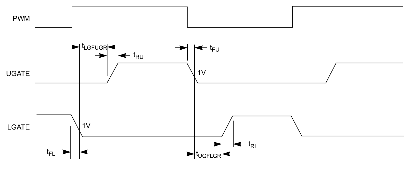
3.6 Gate Driver Timing Diagrams
Figure 6. Gate Driver Timing Diagram