10 KiB
and system voltage VSYS duty cycle ratio. The system bus voltage is regulated at the voltage set on the MaxSystemVoltage register. If the charge current register is programmed (non-zero), the RAA489118 charges the battery either in Trickle Charging mode or Fast Charging mode, as long as BATGONE is low.
9. General Application Information
This design guide provides a high-level explanation of the steps necessary to design a single-phase power converter. It is assumed that the reader is familiar with many of the basic skills and techniques referenced in the following sections. In addition to this guide, Renesas provides complete reference designs that include schematics, bill of materials, and example board layouts.
9.1 Selecting the LC Output Filter
The duty cycle of an ideal buck converter in CCM is a function of the input and the output voltage. This relationship is written by Equation 2:
(EQ. 2)
D = \frac{V_{OUT}}{V_{IN}}Use Equation 3 to calculate the output inductor peak-to-peak ripple current:
(EQ. 3)
I_{P\text{-}P} = \frac{V_{OUT} \bullet (1 - D)}{f_{SW} \bullet L}A typical step-down DC/DC converter has an IP-P of 20% to 40% of the maximum DC output load current for a practical design. The value of IP-P is selected based on several criteria such as MOSFET switching loss, inductor core loss, and the resistive loss of the inductor winding.
Use Equation 4 to estimate the DC copper loss of the inductor, where ILOAD is the converter output DC current.
(EQ. 4)
P_{COPPER} = I_{LOAD}{}^{2} \bullet DCRThe copper loss can be significant, so select DCR carefully. Another factor to consider when choosing the inductor is its saturation characteristics at elevated temperatures. A saturated inductor can destroy circuit components.
A DC/DC buck regulator must have output capacitance CO into which ripple current IP-P can flow. Current IP-P develops a corresponding ripple voltage VP-P across CO, which is the sum of the voltage drop across the capacitor ESR and of the voltage change stemming from charge moved in and out of the capacitor. Use Equation 5 and Equation 6 to calculate these two voltages:
(EQ. 5)
\Delta V_{ESR} = I_{P\text{-}P} \bullet ESR(EQ. 6)
\Delta V_{C} = \frac{I_{P\text{-}P}}{8 \bullet C_{O} \bullet f_{SW}}If the output of the converter has to support a load with high pulsating current, several capacitors need to be paralleled to reduce the total ESR until the required VP-P is achieved. The inductance of the capacitor can cause a brief voltage dip if the load transient has an extremely high slew rate. Low inductance capacitors should be considered in this scenario. A capacitor dissipates heat as a function of RMS current and frequency. Ensure that IP-P is shared by a sufficient quantity of paralleled capacitors so that they operate below the maximum rated RMS current at fSW. Take into account that the rated value of a capacitor can fade as much as 50% as the DC voltage across it increases.
9.2 Selecting the Input Capacitor
The important parameters for input capacitance are the voltage rating and the RMS current rating. For reliable operation, select capacitors with voltage and current ratings above the maximum input voltage and that are capable of supplying the RMS current required by the switching circuit. Their voltage rating should be at least 1.25x greater than the maximum input voltage, while a voltage rating of 1.5x is a preferred rating. Figure 48 is a graph of the input capacitor RMS ripple current that is normalized relative to output load current. The graph is also a function of duty cycle and is adjusted for converter efficiency.
Figure 48. Normalized RMS Input Current at EFF = 1
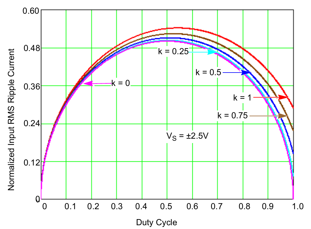
Use Equation 7 to calculate the normalized RMS ripple current calculation:
(EQ. 7)
I_{C_{IN}(RMS,NORMALIZED)} = \frac{I_{MAX} \cdot \sqrt{D \cdot (1 - D) + \dfrac{D \cdot k^{2}}{12}}}{I_{MAX}}where:
- IMAX is the maximum continuous ILOAD of the converter
- k is a multiplier (0 to 1) corresponding to the inductor peak-to peak ripple amplitude expressed as a ratio of IMAX (0 to 1)
- D is the duty cycle that is adjusted to take into account the efficiency of the converter, which is calculated using Equation 8:
(EQ. 8)
D = \frac{V_{OUT}}{V_{IN} \cdot EFF}In addition to the capacitance, some low ESL ceramic capacitance is recommended to decouple between the drain of the high-side MOSFET and the source of the low-side MOSFET.
9.3 Selecting the Switching Power MOSFET
Typically, a MOSFET cannot tolerate even brief excursions beyond its maximum drain-to-source voltage rating. The MOSFETs used in the power stage of the converter should have a maximum VDS rating that exceeds both the sum of the upper voltage tolerance of the input power source and the voltage spike that occurs when the MOSFET switches off.
Several power MOSFETs that are optimized for DC/DC converter applications are readily available. The preferred high-side MOSFET emphasizes low gate charge so that the device spends the least amount of time dissipating power in the linear region. Unlike the low-side MOSFET, which has the drain-to-source voltage clamped by its body diode during turn off, the high-side MOSFET turns off with a VDS of approximately VIN - VOUT, plus the
spike across it. The preferred low-side MOSFET emphasizes low rDS(ON) when fully saturated to minimize conduction loss. Note: This is an optimal configuration of MOSFET selection for low duty cycle applications (D < 50%). For higher output, low input voltage solutions, a more balanced MOSFET selection for high-side and low-side devices might be required.
The power loss of the Low-Side (LS) MOSFET can be assumed to be conductive only and is calculated using Equation 9:
(EQ. 9)
P_{CON\_LS} \approx I_{LOAD}{}^{2} \cdot r_{DS(ON)\_LS} \bullet (1 - D)Use Equation 10 to calculate the conduction loss of the High-Side (HS) MOSFET:
(EQ. 10)
P_{CON\_HS} = I_{LOAD}{}^{2} \bullet r_{DS(ON)\_HS} \bullet DUse Equation 11 to calculate the switching loss of the HS MOSFET:
(EQ. 11)
P_{SW\_HS} = \frac{V_{IN} \bullet I_{VALLEY} \bullet t_{SWON} \bullet f_{SW}}{2} + \frac{V_{IN} \bullet I_{PEAK} \bullet t_{SWOFF} \bullet f_{SW}}{2}where:
- IVALLEY is the difference of the DC component of the inductor current minus 1/2 of the inductor ripple current
- IPEAK is the sum of the DC component of the inductor current plus 1/2 of the inductor ripple current
- tSW(ON) is the time required to drive the device into saturation
- tSW(OFF) is the time required to drive the device into cut-off
9.4 Selecting the Bootstrap Capacitor
The selection of the bootstrap capacitor is written by Equation 12:
(EQ. 12)
C_{BOOT} = \frac{Q_{g}}{\Delta V_{BOOT}}where:
- Qg is the total gate charge required to turn on the high-side MOSFET
- ∆VBOOT is the maximum allowed voltage decay across the boot capacitor each time the high-side MOSFET is switched on.
As an example, suppose the HS MOSFET has a total gate charge Qg, of 25nC at VGS = 5V and a ∆VBOOT of 200mV. The calculated bootstrap capacitance is 0.125µF; for a comfortable margin, select a capacitor that is double the calculated capacitance. In this example, 0.22µF is sufficient. Use an X7R or X5R ceramic capacitor. Renesas recommends using a bootstrap capacitor of 0.47µF (25V), which has an effective capacitance higher than 0.25µF at 5V and x50 effective high-side MOSFET gate capacitance.
9.5 Switching Power MOSFET Gate Capacitance
The RAA489118 includes an internal 5V LDO output at the VDD pin, which can be used to provide the switching MOSFET gate driver power through the VDDP pin with an RC filter. The 5V LDO output overcurrent protection threshold is 85mA, minimal (check EC table for the accurate value). When selecting the switching power MOSFET, consider the MOSFET gate capacitance carefully to avoid overloading the 5V LDO, especially in Buck-Boost mode when four MOSFETs are switching at the same time. For one MOSFET, use Equation 13 to estimate the gate drive current:
(EQ. 13)
I_{driver} = Q_{g} \bullet f_{SW}where:
- Qg is the total gate charge, which can be found in the MOSFET datasheet
- fSW is the switching frequency
Renesas recommends using a 2.2µF (10V) VDD/VDDP capacitor, which has an effective capacitance higher than 0.4µF at 5V and x1.6 effective capacitance at the BOOT pin at 5V.
9.6 DCIN Filter
An RC filter is connected at the DCIN pin. Renesas recommends connecting a 10Ω DCIN resistor between the DCIN pin and the VADP/VSYS diodes, and connecting a 4.7µF DCIN capacitor to GND, which has an effective capacitance higher than 0.4µF at 28V.
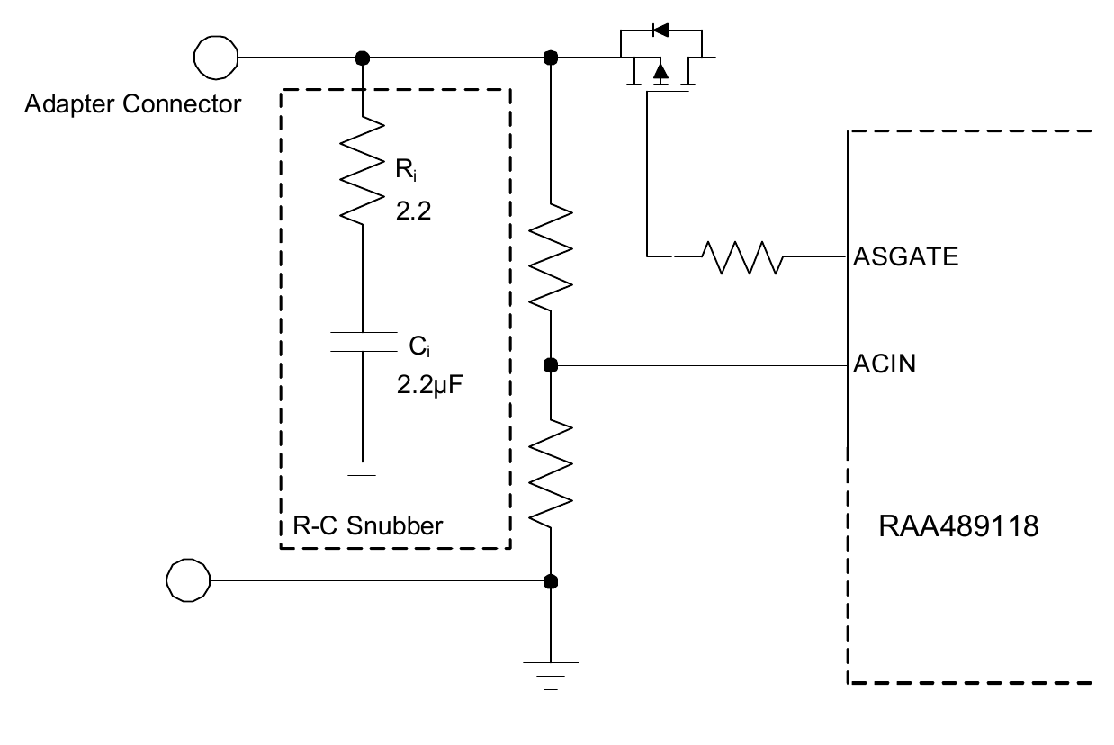
9.7 Adapter Input Filter
The adapter cable parasitic inductance and capacitance can cause some voltage ringing or an overshoot spike at the adapter connector node when the adapter is hot plugged in. This voltage spike can damage the ASGATE MOSFET or the RAA489118 pins connecting to the adapter connector node. One low cost solution is to add an R-C snubber circuit at the adapter connector node to clamp the voltage spike as shown in Figure 49. A practical value of the R-C snubber is 2.2Ω to 2.2µF, while the appropriate values and power rating should be carefully characterized based on the actual design. Renesas does not recommend adding a pure capacitor at the adapter connector node, which can cause an even larger voltage spike due to the adapter cable or the adapter current path parasitic inductance.
Figure 49. Adapter Input R-C Snubber Circuit