
4.2 KiB
4.2 KiB
RAA489400 Datasheet
8. Layout
| Pin # | Pin Name | Layout Guidelines |
|---|---|---|
| 2 | CC1 |
Route the trace with sufficient width. Place decoupling capacitor to filter the noise. Renesas recommends placing the charger CC pins as close to the USB connector as possible, avoid stubs on the CC lines, and route the CC lines with about the same length. |
| 26 | CC2 |
Route the trace with sufficient width. Place decoupling capacitor to filter the noise. Renesas recommends placing the charger CC pins as close to the USB connector as possible, avoid stubs on the CC lines, and route the CC lines with about the same length. |
| 3 | RD1 |
Connect to CC1, if dead battery Rd needs to be supported. |
| 25 | RD2 |
Connect to CC2, if dead battery Rd needs to be supported. |
| 8 | GPIO1 |
Digital pin, open-drain, push-pull output or input. No special consideration. |
| 7 | GPIO2 |
Digital pin, open-drain, push-pull output or input. No special consideration. |
| 6 | GPIO3 |
Digital pin, open-drain, push-pull output or input. No special consideration. |
| 5 | GPIO4 |
Digital pin, open-drain, push-pull output or input. No special consideration. |
| 9 | OCP# |
Digital pin, open-drain output. No special consideration. |
| 20 | SNK_DISCHG |
Run a dedicated trace from the internal sink power rail to the pin. |
| 32 | PROCHOT# |
Digital pin, open-drain output. No special consideration. |
| 10 | PROG |
Signal pin. Place the PROG programming resistor in the general proximity of the controller. |
| 29 | SDA |
Digital pins. No special consideration. Run the SDA and SCL traces in parallel. |
| 28 | SCL |
Digital pins. No special consideration. Run the SDA and SCL traces in parallel. |
| 31 | ALERT# |
Digital pin, open-drain output. No special consideration. |
| 19 | VSNK_SRC |
Run this trace with sufficient width in parallel fashion with the VSNK_GATE trace. |
| 18 | VSNK_GATE |
Run this trace with sufficient width in parallel fashion with the VSNK_SRC trace. |
| 22 | VSRC_SRC |
Run this trace with sufficient width in parallel fashion with the VSRC_GATE trace. |
| 21 | VSRC_GATE |
Run this trace with sufficient width in parallel fashion with the VSRC_SRC trace. |
| 23 | VSRC_BOOT |
Connect to VSRC_SRC through a capacitor. |
| 16 | CSIN |
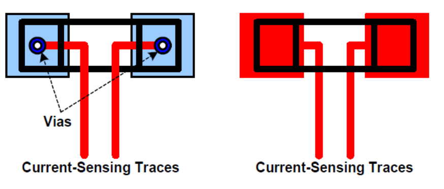
Run two dedicated traces with sufficient width in parallel (close to each other to minimize the loop area) from the two terminals of the adapter current-sensing resistor to the IC. Place the Differential mode and common-mode RC filter components in the general proximity of the controller. Route the current-sensing traces through vias to connect the center of the pads or route the traces into the pads from the inside of the current-sensing resistor. The following drawings show the two preferred ways of routing current-sensing traces. |
| 15 | CSIP |
Run two dedicated traces with sufficient width in parallel (close to each other to minimize the loop area) from the two terminals of the adapter current-sensing resistor to the IC. Place the Differential mode and common-mode RC filter components in the general proximity of the controller. Route the current-sensing traces through vias to connect the center of the pads or route the traces into the pads from the inside of the current-sensing resistor. The following drawings show the two preferred ways of routing current-sensing traces. |
| 14 | VBUS |
Run a dedicated trace from the VBUS to the pin. |
| 12 | VSYS33 |
Run a dedicated trace from the system to the pin. |
| 30 | VCONN_POWER |
Place the decoupling capacitor in the general proximity of the controller. Route the trace with sufficient width. |
| 13 | VDD33 |
Place the decoupling capacitor in the general proximity of the controller. Route the trace with sufficient width. |
| 4 | VDD25 |
Place the decoupling capacitor in the general proximity of the controller. Route the trace with sufficient width. |
| 24 | GND |
Connect this pin to the ground plane. |
| 1, 7, 17, 23 | NC |
No connection. Although open, soldering is required. |
R16DS0292EU0100 Rev.1.00 Aug 27, 2024
Page 79