
66 KiB
Chapter 4. Power Delivery Electrical Requirements
Throughout this chapter, certain functionally equivalent electrical parameters are identified by different names depending on the Contract type (Fixed, AVS, PPS etc.), though their behavior is consistent across Contract type. To standardize terminology and reduce redundancy, the following table defines a set of aliases mapped to specific variables. The aliases will be used throughout this chapter and will collectively refer to each of the parameters it is aliasing. For example, any figure using the vNew alias represents an equivalent figure for vSrcNew, vAvsNew, and vPpsNew. The alias will not be used where the behavior does not apply to all aliased parameters.
Table 4.1. Universal Aliases for PDO or APDO Variables
| Alias | Fixed PDO Parameter | AVS APDO Parameter | PPS APDO Parameter |
|---|---|---|---|
iSlewNeg |
iLoadReleaseRate |
iLoadReleaseRate |
iLoadReleaseRate or iPpsCLLoadReleaseRate |
iSlewPos |
iLoadStepRate |
iLoadStepRate |
iLoadStepRate or iPpsCLLoadStepRate |
tSrcTransLarge |
-- | tAvsSrcTransLarge |
tPpsSrcTransLarge |
tSrcTransSmall |
-- | tAvsSrcTransSmall |
tPpsSrcTransSmall |
tTransient |
tSrcTransient |
tAvsTransient |
tPpsTransient |
vMaxVoltage |
-- | vAvsMaxVoltage |
vPpsMaxVoltage |
vMinVoltage |
-- | vAvsMinVoltage |
vPpsMinVoltage |
vNew |
vSrcNew |
vAvsNew |
vPpsNew |
vSlewNeg |
vSrcSlewNeg |
vAvsSlewNeg |
vPpsSlewNeg |
vSlewPos |
vSrcSlewPos |
vAvsSlewPos |
vPpsSlewPos |
vSmallStep |
vAvsSmallStep |
vPpsSmallStep |
|
vStep |
-- | vAvsStep |
vPpsStep |
vValid |
vSrcValid |
vAvsValid |
vPpsValid |
4.1. Source Requirements
4.1.1. Behavioral Aspects
A USB PD Source is a device that supplies power over a USB connection using the USB Power Delivery protocol. It advertises available voltage and current levels, negotiates power contracts with Sinks, and adjusts its output accordingly. In addition to being a USB Type-C Source and following all [USB-C] defined behaviors, a USB PD Source must meet all requirements defined in this chapter.
4.1.2. Source Bulk Capacitance
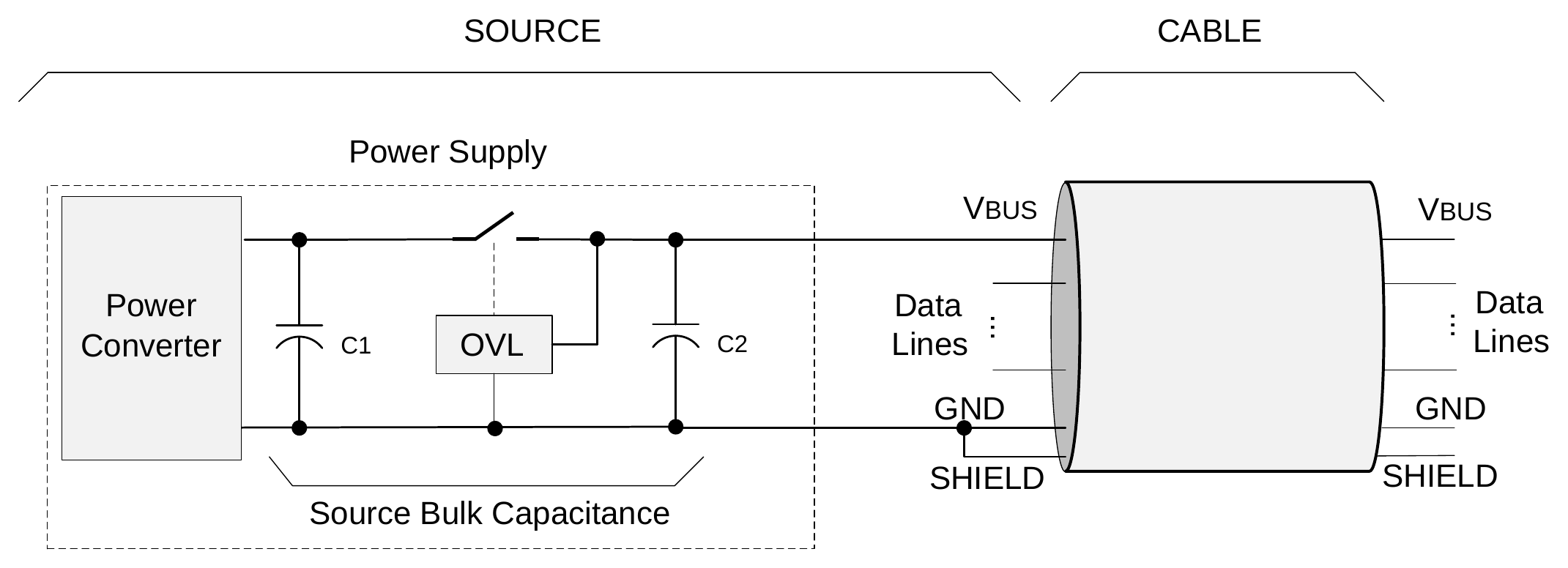
The Source bulk capacitance consists of C1 and C2 as shown in. The switch (or Ohmic Interconnect) usually consists of one or two MOSFETs and May be part of the circuit implemented by the Source to control its VBUS Output Voltage Limit (OVL) as described in. The capacitance might be a single capacitor, a capacitor bank or distributed capacitance. If the power supply is dedicated to a single Port, the minimum bulk capacitance is defined as cSrcBulk. If the power supply is shared across multiple ports, the bulk capacitance is defined as cSrcBulkShared.
The Source bulk capacitance is allowed to change for a newly Negotiated power level. The capacitance change Shall occur before the Source is ready to operate at the new power level. During a Power Role Swap, the Initial Source Shall transition to Swap Standby before operating as the New Sink. Any change in bulk capacitance required to complete the Power Role Swap Shall occur during Swap Standby.
Figure 4.1. Placement of Source Bulk Capacitance
4.1.2.1. Source PDOs or APDOs
Consistent with the Power Data Objects discussed in Section 6.4.1.3, the power supply PDO or APDO that are available as a Source in a USB Power Delivery System are:
-
The Fixed Supply PDO exposes well-regulated fixed voltage power supplies. A Source Shall support at least one Fixed Supply PDO providing
vSafe5V. The output voltage of a Fixed Supply Shall remain within the range defined by the relative tolerancevSrcNewand the absolute bandvSrcValidas listed in Table 4.6 and described in Section 4.1.2.1.1 -
The Variable Supply (non-Battery) PDO exposes less well-regulated Sources. The output voltage of a Variable Supply (non-Battery) Shall remain within the absolute maximum output voltage and the absolute minimum output voltage exposed in the Variable Supply PDO.
-
The Battery Supply PDO exposes Batteries that can be Connected directly as a Source to VBUS. The output voltage of a Battery Supply Shall remain within the absolute maximum output voltage and the absolute minimum output exposed in the Battery Supply PDO.
-
The Programmable Power Supply (PPS) and Adjustable Voltage Source (AVS) Augmented Power Data Object (APDO) expose a Source with an output voltage that can be adjusted programmatically over a defined range.
-
For AVS, the output voltage Shall remain within a range defined by the relative tolerance
vAvsNew, and the absolute bandvAvsValid. -
For PPS, the output voltage Shall remain within a range defined by the relative tolerance
vPpsNewand the absolute bandvPpsValid. These limits are applicable as long as Operating Mode Flag (OMF) is 0. See Section 4.1.3.2.2 for OMF information.
-
4.1.2.1.1. Voltage Regulation
This section applies to the Source while operating in any of the PDOs discussed on Section 4.1.2.1.
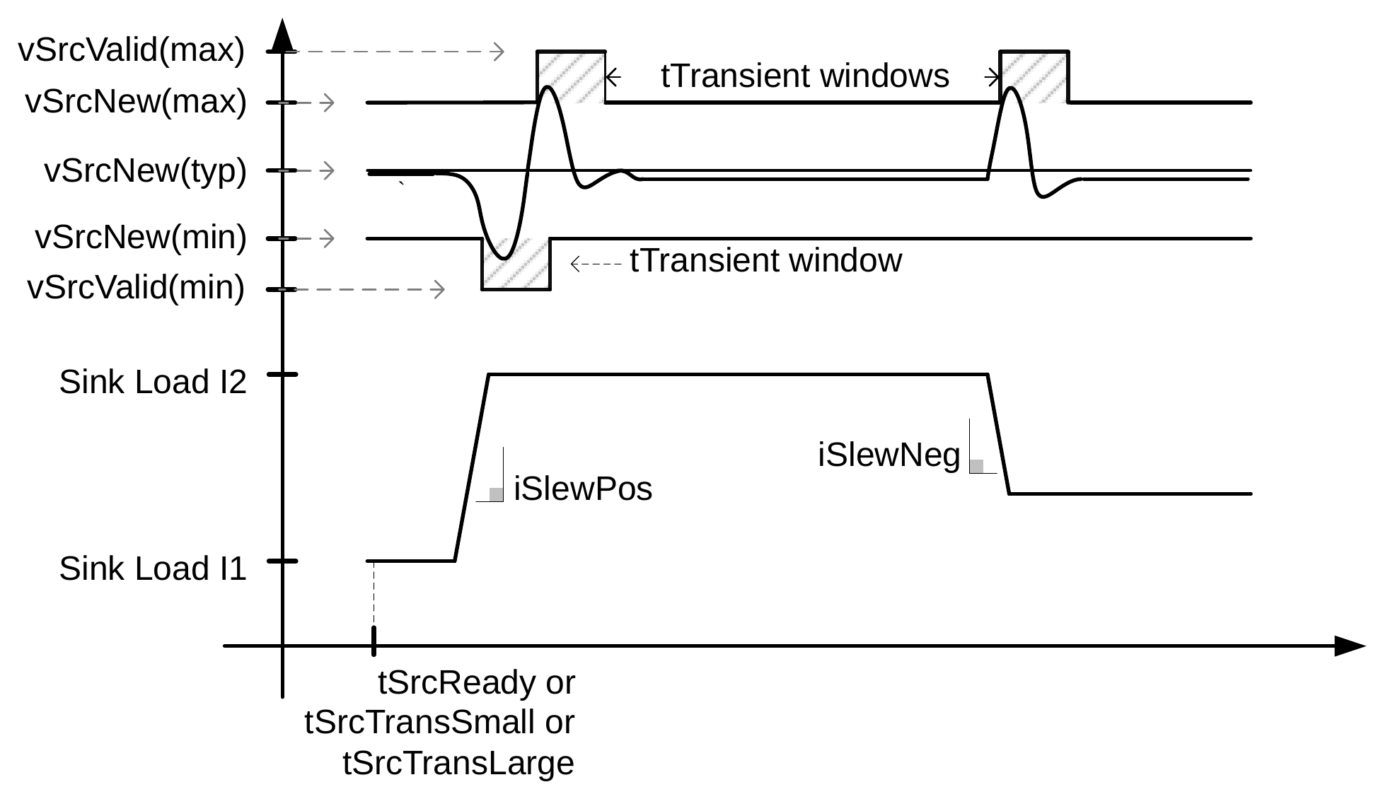
After a voltage transition is complete (i.e., after tSrcReady, tSrcTransSmall or tSrcTransLarge ) and during static load conditions, the Source output voltage Shall remain within the vNew or vSafe5V limits as applicable. The ranges defined by vNew and vSafe5V account for DC regulation accuracy, line regulation, load regulation, and output ripple.
During transient load conditions (defined by iSlewPos or iSlewNeg), the Source output voltage Shall Not go beyond
the range specified by vValid. The amount of time the Source output voltage can be in the band between either vNew or vSafe5V and vValid Shall Not exceed tTransient. Refer to Table 4.6 for the output voltage tolerance specifications. Figure 4.2 illustrates the application of vNew and vValid after the voltage transition is complete.
The vNew and vValid limits Shall Not apply to VBUS during the VBUS discharge and switchover that occurs during a Fast Role Swap as described in Chapter 10.
Figure 4.2. Application of vNew and vValid limits after tSrcReady or tSrcTransSmall or tSrcTransLarge
The Source output voltage Shall be measured at the connector receptacle. The stability of the Source is left to the discretion of the implementer; however, the design Shall account for the possibility that the Sink May introduce any load transient inside the constraints of the Contract, provided that the slew rate is between iSlewPos and iSlewNeg. The transient behavior of the load current is defined in Section 4.2.6.
In some systems it might be necessary to design the Source to compensate for the voltage drop between the output stage of the power supply electronics and the receptacle contact. The determination of whether compensation is necessary is left to the discretion of the Source implementation.
4.1.3. Source Transitions
4.1.3.1. Fixed Voltage Transitions
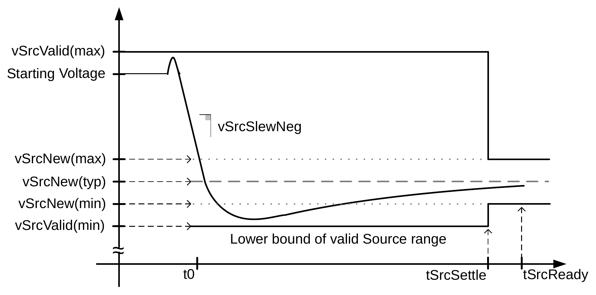
The Source Shall transition VBUS from the starting voltage to the new voltage in a controlled manner. Figure 4.3 and Figure 4.4 illustrate the transition process for positive and negative fixed voltage transitions respectively. The following statements Shall be observed for fixed voltage transitions:
-
The Negotiated new voltage (e.g., 5V, 9V, 15V, …) defines the nominal value for
vSrcNew. -
During the positive transition the Source Shall be able to supply the Sink Standby current and the transient current to charge the total bulk capacitance on VBUS.
-
The slew rate of the positive transition Shall Not exceed
vSrcSlewPosand the slew rate for a negative transition Shall Not exceedvSrcSlewNeg. -
The transitioning Source output voltage Shall settle within
vSrcNewbytSrcSettle. -
The Source Shall be able to supply the Negotiated power level at the new voltage by
tSrcReady. -
Voltage transitions follow these rules:
-
The positive voltage transition Shall remain above
vSrcValid(min) of the previous Explicit Contract and belowvSrcValid(max) of the new Explicit Contract. -
The negative voltage transition Shall remain below
vSrcValid(max) of the previous Contract and abovevSrcValid(min) of the new Explicit Contract.
-
-
The starting time, t0, in Figure 4.3 starts
tSrcTransitionafter the last bit of the EOP of theGoodCRCMessage has been received by the Source. -
Negative transitions to
vSafe0Vdo not have the same requirements illustrated in Figure 4.4. See Section 4.1.5.5.
Figure 4.3. Transition Envelope for Positive Voltage Transitions
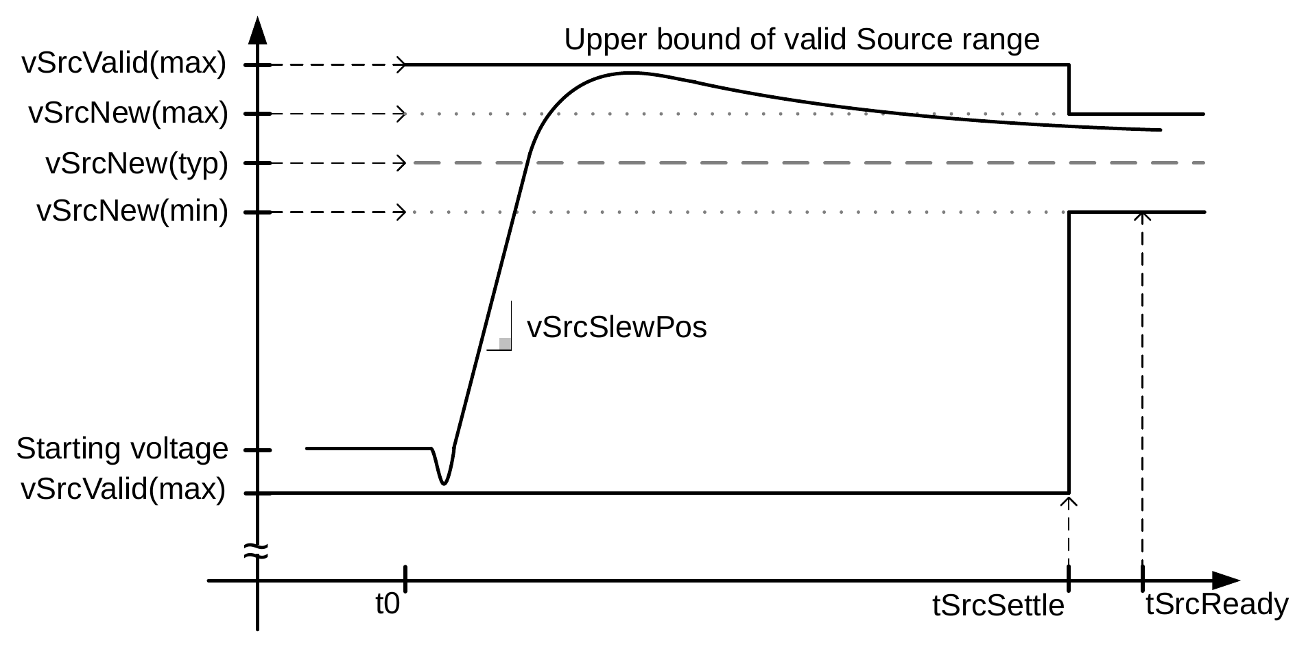
Figure 4.4. Transition Envelope for Negative Voltage Transitions
4.1.3.2. AVS/PPS Transitions
4.1.3.2.1. Voltage Transitions
When in AVS or PPS Mode, the Source Shall transition VBUS over the defined voltage range in a controlled manner. The output voltage in the RDO defines the nominal value of the output voltage after completing a voltage transition. The following statements Shall be observed by an AVS Source and by a PPS Source when not in Current Limit (CL) Mode (see Section 4.1.3.2.2 ):
-
Settle within the limits defined by
vNewbytSrcTransSmallfor steps smaller than or equal tovSmallStep. -
Settle within limits defined by
vNewbytSrcTransLargefor steps larger thanvSmallStep. -
Overshoot and undershoot Shall not exceed
vValid. -
The voltage May change in a step-wise or linear manner and the slew rate of either type of change Shall Not exceed
vSlewPosfor voltage increases orvSlewNegfor voltage decreases. -
The nominal requested voltage equates to an integer number of LSB changes, which are defined as
vStep. -
If an increase in voltage is requested, then the new voltage Shall be greater than or equal to the current voltage. See Section 4.1.3.2.6 for more details.
-
If a decrease in voltage is requested, then the new voltage Shall be less than or equal to the current voltage. See Section 4.1.3.2.6 for more details.
-
The voltage range is defined by the parameters
vMinVoltageandvMaxVoltage, corresponding to the Minimum Voltage and Maximum Voltage fields of the respective APDOs. Table 4.2 and Table 4.3 show the valid voltage ranges for PPS and SPR AVS.
Table 4.2. SPR Programmable Power Supply (PPS) Voltage Ranges
| Fixed Nominal Voltage | 9V Prog | 15V Prog | 20V Prog |
|---|---|---|---|
| Maximum Voltage | 11V | 16V | 21V |
| Minimum Voltage | 5V | 5V | 5V |
Table 4.3. SPR Adjustable Voltage Supply (AVS) Voltage Ranges
| AVS Voltage Range | 15V | 20V |
|---|---|---|
| Maximum Voltage | 15V | 20V |
| Minimum Voltage | 9V | 9V |
Table 4.4 show the valid voltage ranges for EPR AVS.
Table 4.4. EPR Adjustable Voltage Supply (AVS) Voltage Ranges
| AVS Voltage Range | 28V | 36V | 48V |
|---|---|---|---|
| Maximum Voltage | 28V | 36V | 48V |
| Minimum Voltage | 15V | 15V | 15V |
Figure 4.5 illustrates the output voltage behavior of PPS and an AVS Source in response to positive and negative voltage change requests.
Figure 4.5. PPS/AVS Voltage Transitions

While in PPS Mode and in the specific case of CL operation (see Section 4.1.3.2.2 ), the voltage might not change to a new requested level, since in this Mode it is the current that is being controlled by the Source (e.g., when the
Sink is directly charging a Battery from VBUS). Note: the Source cannot rely on checking the voltage on VBUS to determine when its power supply is ready to send a PS_RDY Message.
If the Sink negotiates for a new PDO or APDO, then the transition between the current PDO or APDO and the new PDO or APDO Shall occur as described in Section 4.5.
Section 4.1.4 lists transitions that are exempt from the vSlewNeg and vSlewPos limits.
See Section 4.1.3.2.5 for output voltage ripple limits.
See Section 4.1.3.2.6 for output voltage and current DNL step adjustments.
4.1.3.2.2. PPS Operation in Current Limit (CL) Mode
The Programmable Power Supply operating in PPS Mode Current Limit (CL) Mode Shall observe the following:
-
If the Sink attempts to draw current exceeding the Operating Current specified in the RDO, the Source Shall limit its output to a level within the tolerance defined by
iPpsCLNew. -
The programming step size for the Operating Current is
iPpsCLStep, and whenever a new current is requested, the settling time istPpsCLProgramSettle. -
The Current Limit programmability ranges from
iPpsCLMinand the Maximum Current value in the PPS APDO.-
A Source which receives a Request for current below
iPpsCLMinShould reject the Request. -
A Source that accepts a Request for current below
iPpsCLMinShall set its Current Limit at 1A.
-
-
A PPS Source that is operating in Current Limit Shall Not change its set-point in a manner that exceeds
iPpsCLLoadStepRateoriPpsCLLoadReleaseRate. -
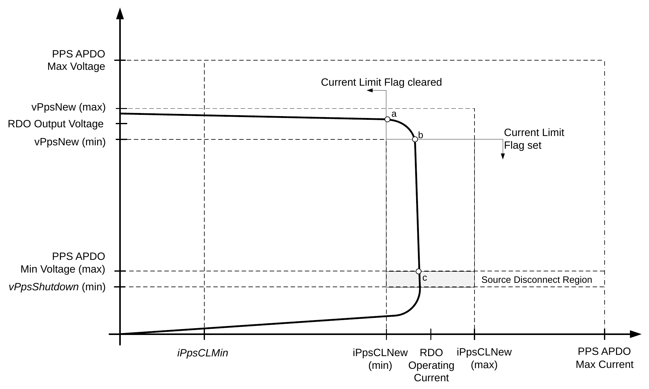
If during CL Mode, the output voltage drops below
vPpsShutdownthe Source May send a Hard Reset and Shall discharge VBUS tovSafe0V, then resume USB Default Operation atvSafe5V. -
The Source Shall Not shut down or otherwise disrupt the available output power while in Current Limit Mode unless another protection mechanism as outlined in Section 4.1.5 is engaged to protect the Source from damage.
The response of a PPS to a load change depends on the Operating Mode of the PPS and the magnitude of the load change. These dependencies lead to one of four possible responses of a PPS to any load change as shown in. They are differentiated by the value of the PPS Status OMF (see Section 6.5.13), in the initial and final State of the load change.
Table 4.5. PPS Status
| OMF Initial | OMF Final | Operation |
|---|---|---|
| 0 | 0 | Output Voltage maintained, transient range allowed as shown in insert Figure 4.6 |
| 0 | 1 | At the end of the transient, the feedback loop of the Source controls the VBUS Current, as opposed to the voltage, which is determined by the Sink (usually by the Sink's Battery). The Current Shall settle within iPpsCLNew by tPpsCVCLTransient. During the transient itself the Current is allowed to be within iPpsCVCLTransient. |
| 1 | 0 | At the end of the transient, the feedback loop of the Source controls the VBUS Voltage, as opposed to the current. During the transient the voltage Shall stay within vPpsCLCVTransient. After tPpsCLCVTransient the VBUS voltage Shall be within vPpsNew. |
| 1 | 1 | Output Current maintained. The transient range allowed is extended by iPpsCLTransient, and the settling time is tPpsCLSettle. After this period the allowed range is iPpsCLNew. |
The relationship between PPS programmable output voltage and PPS programmable Current Limit is as shown in. The transition between the Constant Voltage Mode and the Current Limit Mode occurs between points a and b. The PPS Status OMF Shall be set or cleared within this region. When VBUS falls below the APDO Minimum Voltage (point c), the Source is allowed to disconnect.
Figure 4.6. PPS Programmable Voltage and Current Limit
4.1.3.2.3. PPS Operation in Constant Power
The tolerances along the Constant Power Curve Shall Not extend into the Guaranteed Capability Area shown in Figure 4.7 as the region inside the dashed line defined by PPS APDO Minimum Voltage (max), vPpsNew (min), and iPpsCLNew (min).
Figure 4.7. PPS Constant Power
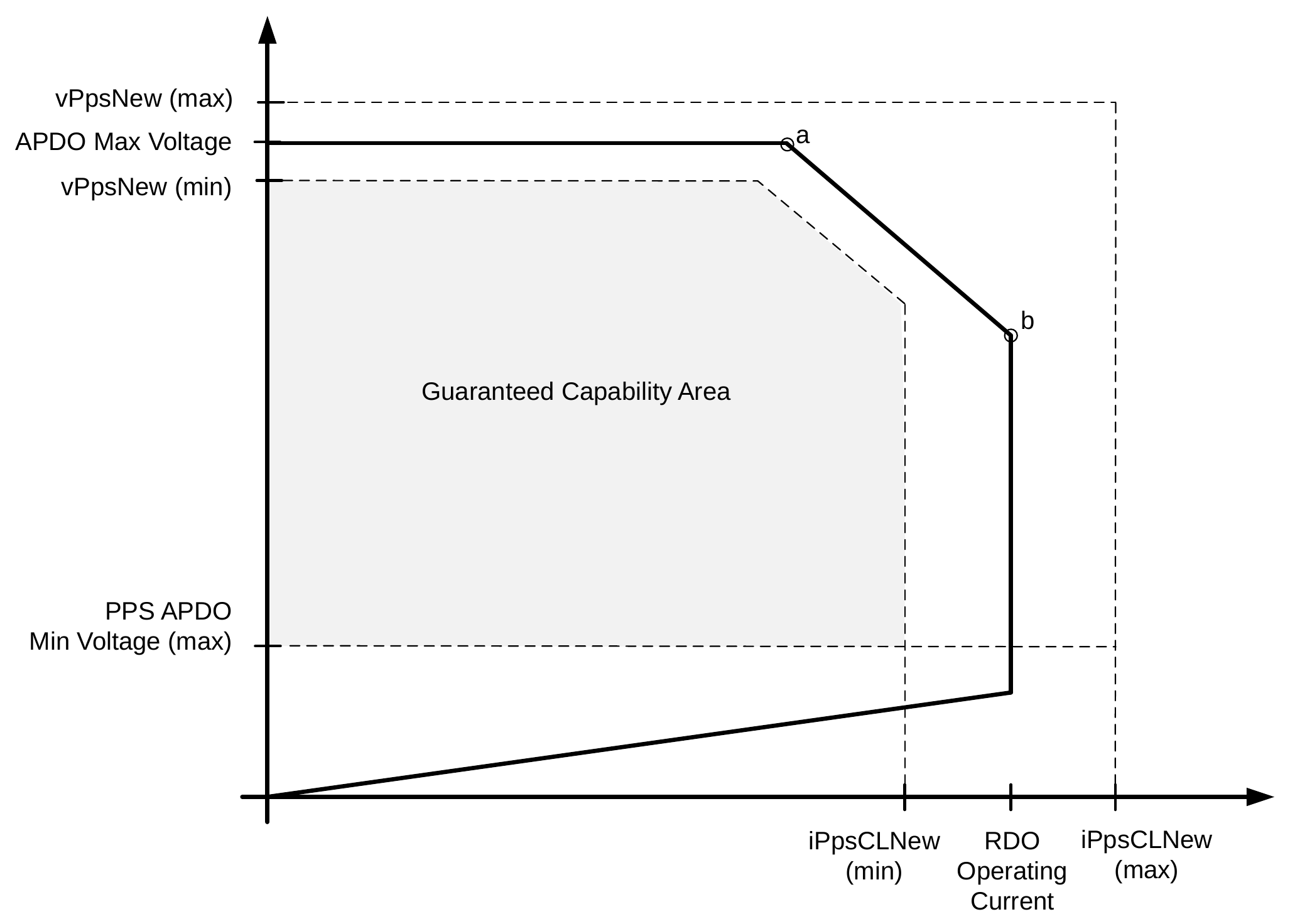
In the example above, the section between points a and b represents the constant power area of the CV/CL curve.
4.1.3.2.4. Adjustable Voltage Supply Source Current
Unless otherwise noted, AVS Shall follow the same requirements as a Fixed Supply.
The maximum operating current the AVS shall supply is determined as follows:
- For SPR AVS APDOs, the maximum operating current is defined in the Maximum Current field of the 15V AVS APDO and the 20V AVS APDO in the SPR Source_Capabilities Message.
- For EPR AVS APDOs, the maximum operating current is calculated as the lower of the ((PDP field value) ÷ (Output Voltage)) or 5A whichever is lower. See Table 3.5.
4.1.3.2.5. Source AVS/PPS Ripple
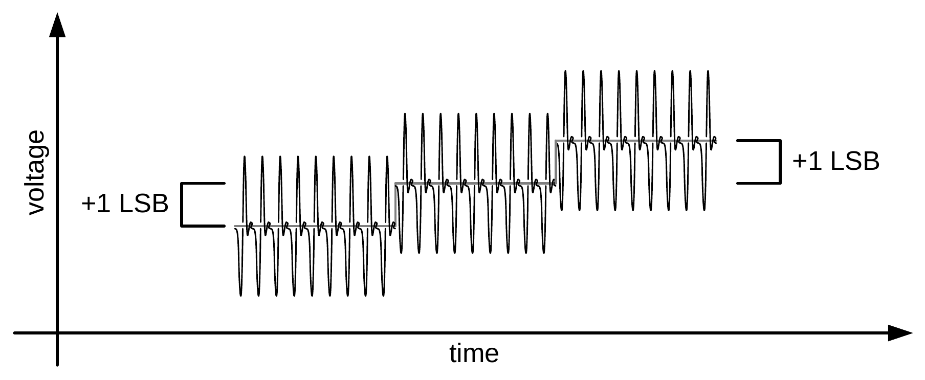
The AVS/PPS output voltage ripple is expected to exceed the magnitude of one or more LSB as shown in the Figure 4.8.
Figure 4.8. Expected PPS Ripple Relative to an LSB
4.1.3.2.6. Source DNL Tolerance
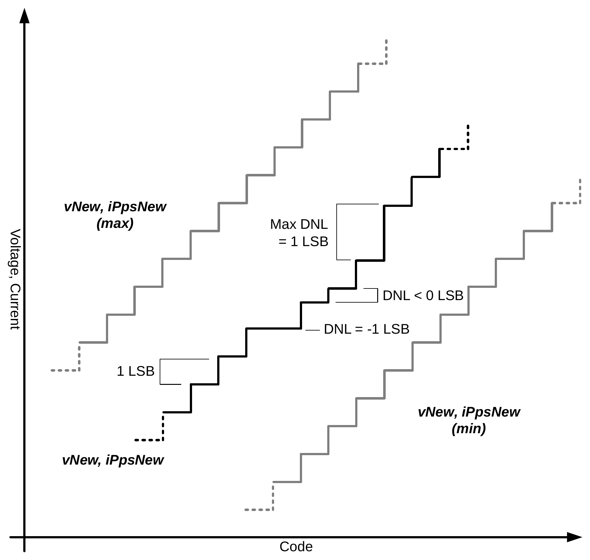
The PPS voltage and current discrete LSB steps have a DNL tolerance as shown in Figure 4.9. In absolute terms the step size of the LSB for both voltage and current is defined by vPpsStep / vAvsStep for voltage and iPpsCLStep for current. Several examples of Valid LSB steps are shown in Figure 4.9:
- The upper end of the DNL error (+1 LSB) shows the case where one step is effectively skipped.
- The lower end of the DNL error (-1 LSB) shows the case where the voltage or current set-point remained the same.
The ideal DNL is 0 LSB where the voltage or current step is exactly equal to the defined LSB step size.
The intent of DNL is to guarantee that changes to the voltage/current have the correct directionality, and that the maximum step size is clearly defined.
Note: The Source Should avoid scenarios where multiple consecutive steps have errors close to the Maximum and Minimum DNL.
Figure 4.9. Allowed DNL Errors and Tolerance of Voltage and Current in AVS/PPS Mode
4.1.4. Non-application of VBUS Slew Rate Limits
Scenarios where vSrcSlewPos and vPpsSlewPos VBUS slew rate limits do not apply and VBUS May transition faster than specified are as follows:
- When first applying VBUS after an Attach.
- When applying VBUS as part of a Power Role Swap to Source Power Role.
- When increasing VBUS from vSafe0V to vSafe5V during a Hard Reset.
- During a Fast Role Swap when the Initial Sink applies VBUS.
- When discharging VBUS to vSafe0V during a Hard Reset.
- When discharging VBUS to vSafe0V as part of a Power Role Swap to Sink Power Role.
- When discharging VBUS to vSafe0V after a Detach.
- During a Fast Role Swap when the VBUS power Source Connected to the Hub UFP stops sourcing power.
4.1.5. Robust Source Operation
4.1.5.1. Output Over-Current Protection
A Source Shall implement Over-Current Protection (OCP) in accordance with the applicable safety standards. The over-current protection May be dynamic depending on the Contract established with the Sink, but it Shall Not activate if the current being drawn is valid per the current Contract.
A Source Should attempt to send Hard Reset Signaling when OCP engages followed by an Alert Message indicating an OCP event when an Explicit Contract has been established. The over-current protection response May engage at either the Port or system level. Systems or ports that have engaged over-current protection Should attempt to resume USB Default Operation.
The Source Shall renegotiate with the Sink after choosing to resume USB Default Operation. The decision of how to renegotiate after an over-current event is left to the discretion of the Source implementation.
During the over-current response and subsequent system or Port shutdown, all affected Source ports operating with VBUS greater than vSafe5V Shall discharge VBUS to vSafe5V within tSafe5V and vSafe0V within tSafe0V.
4.1.5.2. Output Over-Voltage Protection
Over-voltage protection (OVP) is left to the Source implementation to meet any applicable safety or reliability standards. Any OVP Shall account for vNew and vValid when establishing the threshold for OVP, irrespective of the type of Contract that is established with the Sink.
4.1.5.3. Over-Temperature Protection
A Source Should implement Over-Temperature Protection (OTP) to prevent damage from temperature that exceeds the thermal capability of the Source. The definition of thermal capability and the monitoring locations used to trigger the OTP are left to the discretion of the Source implementation.
In order to avoid reaching an OTP event, a Source May proactively reduce the available power being offered to the Sink, even though this might be lower than the Source would be expected to offer during normal thermal operating conditions. Prior to reducing power, the Source Should generate an Alert Message indicating an Operating Condition Change and set the Temperature Status bit in the SOP Status Message to Warning (10b).
A Source Should attempt to send Hard Reset Signaling when OTP engages followed by an Alert Message indicating an OTP event once an Explicit Contract has been established. The OTP response May engage at either the Port or system level. Systems or ports that have engaged OTP Should attempt to resume USB Default Operation and May latch off to protect the Port or system.
The Source Shall renegotiate with the Sink after choosing to resume USB Default Operation. The decision of how to renegotiate after an over-temperature event is left to the discretion of the Source implementation.
During the OTP and subsequent system or Port shutdown, all affected Source ports operating with VBUS greater than vSafe5V Shall discharge VBUS to vSafe5V within tSafe5V and vSafe0V within tSafe0V.
4.1.5.4. vSafe5V Externally Applied to Ports Supplying vSafe5V
A Power Delivery Source Shall be tolerant of vSafe5V being present on VBUS when simultaneously applying power to VBUS. Normal USB PD communication Shall be supported when this vSafe5V to vSafe5V connection exists.
4.1.5.5. Detach
A USB Detach is detected electrically using CC detection on the USB Type-C connector. When the Source is Detached, the Source Shall transition to vSafe0V within tSafe0V from when the Detach event occurred. During the transition to vSafe0V, the VBUS voltage Shall be below vSafe5V (max) within tSafe5V from when the Detach event occurred and Shall Not exceed vSafe5V max after this time.
Note: A USB-PD transmission by the Source during a disconnect event will delay disconnect detection by the Source.
4.1.6. Source Peak Current Operation
A Source that has the Fixed Supply PDO or AVS APDO Peak Current bits set Shall be designed to support one of the overload Capabilities defined in Table 6.18 respectively. The overload conditions are bound in magnitude, duration and duty cycle. When overload conditions occur, the Source is allowed the range of vSrcPeak (instead of vNew ) relative to the nominal value. See Figure 4.10. Note: A Source operating in PPS Mode cannot support peak currents, due to the CL requirements.
Figure 4.10. Source Peak Current Overload
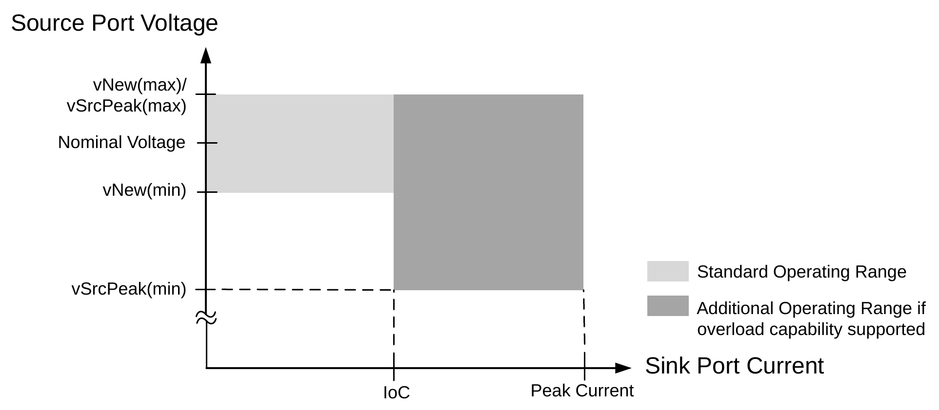
Each overload period Shall be followed by a period of reduced current draw such that the rolling average current over the Overload Period field value with the specified Duty Cycle field value (see Section 6.4.1.3.13 ) Shall Not exceed the Negotiated current. This is calculated as:
Period of reduced current = (1 - (value in Duty Cycle field ÷100)) × value in Overload Period field
The Source May send a New Source_Capabilities Message with the Fixed Supply PDO or AVS APDO Peak Current bits set to 00b to prohibit overload operation even if an overload capability was previously Negotiated with the Sink.
4.1.7. Source Capabilities Extended Parameters
Implementers can choose to make available certain characteristics of a Source Port as a set of Static and/or dynamic parameters to improve interoperability between external power sources and portable computing devices. The complete list of reportable Static parameters is described in full in. The following section offers additional details on some specific electrical parameters.
4.1.7.1. Load Step Slew Rate
The default load step slew rate is established at 150mA/µs. A Source Shall meet the following requirements under the load step reported in the Source_Capabilities_Extended Message:
- The Source Shall maintain VBUS regulation within the vValid range.
- The noise on the CC line Shall remain below vNoiseIdle and vNoiseActive.
Test conditions require a change in both positive and negative load steps from 1Hz to 5000Hz, up to the Advertised Load Step Magnitude of the full load output including from both 10 mA and 10% initial load. The Source Shall ensure that PD Communications meet the transmit and receive masks as specified in Section 5.3.4.1 and Section 5.3.4.2 under all load conditions.
4.1.7.2. Load Step Magnitude
The default load step magnitude rate Shall be 25% of IoC. The Source May report higher capability, tolerating a load step of 90% of IoC.
4.1.7.3. Holdup Time Field
The Holdup Time field Shall return a numeric value of the number of milliseconds the output voltage stays in regulation upon a short interruption of the AC Supply.
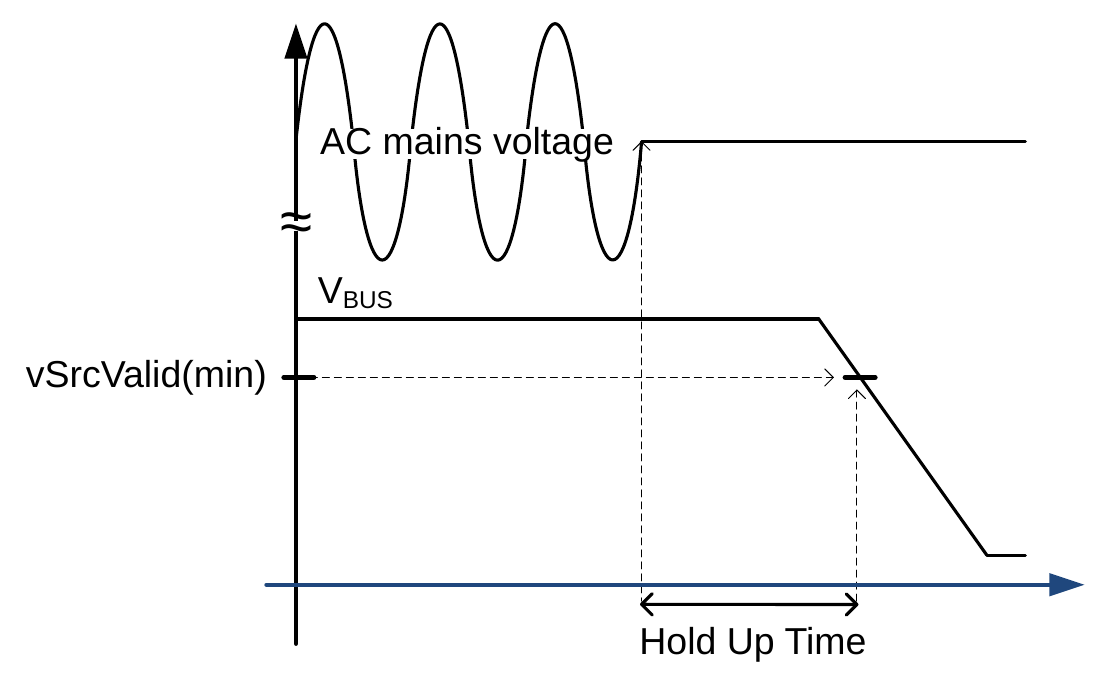
An AC Supplied Source Shall report its holdup time in this field. The holdup time is measured with the load at rated maximum, with the AC Supply at 115VAC rms and 60Hz (or at 230VAC rms and 50Hz for a Source that does not support 115VAC AC Supply). The reported time describes the minimum length of time from the last completed AC Supply input cycle (zero-degree phase angle) until when the output voltage decays below vSrcValid (min). A Source is recommended to support a minimum of 3ms and is preferred to support over 10 milliseconds holdup time (equivalent to a half cycle drop from the AC Supply). See Figure 4.11.
Figure 4.11. Holdup Time Measurement
4.1.7.4. Compliance Field
An SPR Source claiming LPS, PS1 or PS2 compliance (see [IEC 60950-1] and [IEC 62368-1]) Shall report its Capabilities in the Compliance field.
4.1.7.5. Batteries
The Number of Batteries/Battery Slots field Shall report the number of Batteries the Source supports. The Source Shall independently report the number of Hot Swappable Batteries and the number of Fixed Batteries.
4.2. Sink Requirements
4.2.1. Behavioral Aspects
A USB PD Sink is a Device that receives power over a USB connection using the USB Power Delivery protocol. It monitors available power from the Source, requests specific voltage and current levels, and manages its power consumption based on the Negotiated Contract. In addition to being a USB Type-C Sink and following all [USB-C] defined behaviors, a USB PD Sink must meet all requirements defined in this chapter.
4.2.2. Sink Bulk Capacitance
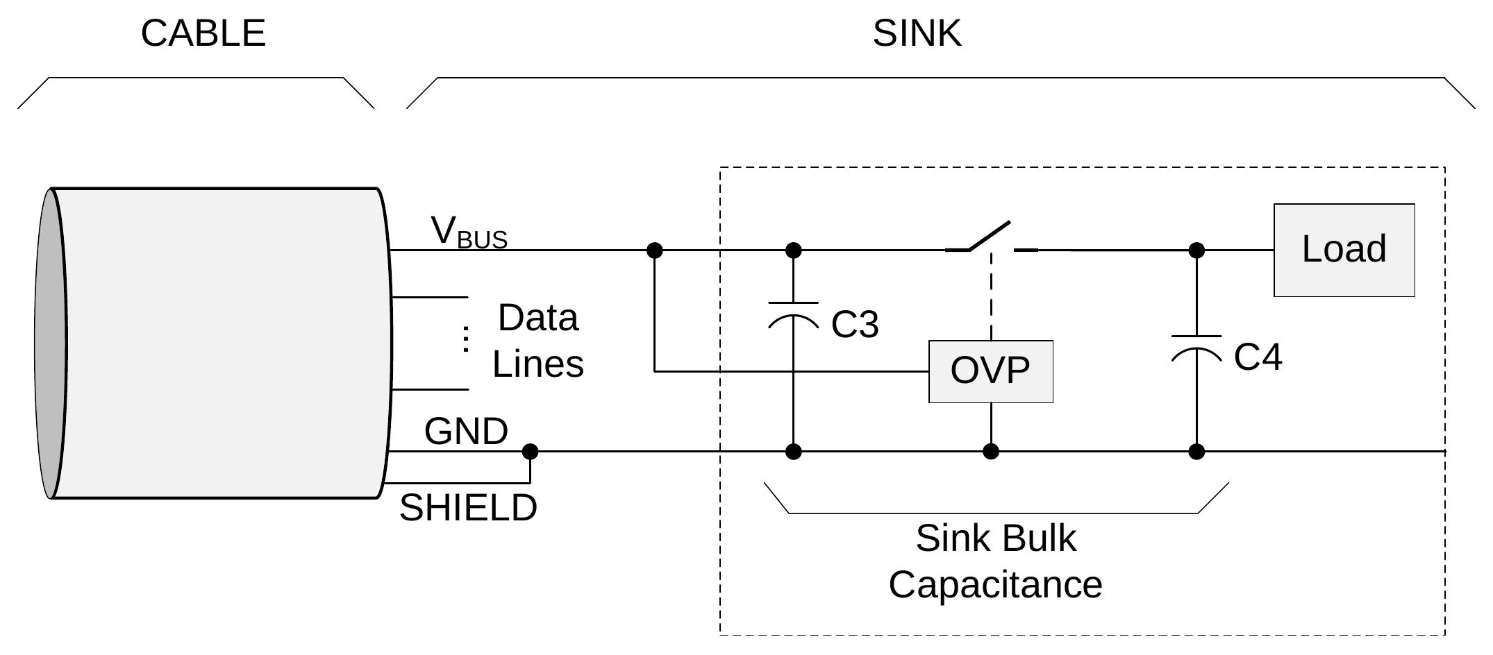
The Sink bulk capacitance consists of C3 and C4 as shown in Figure 4.12. The Ohmic Interconnect might consist of PCB traces for power distribution or power switching devices. The Ohmic Interconnect is expected to be part of an input Over-Voltage Protection (Sink OVP) circuit implemented by the Sink as described in Section 4.1.5.2 to protect against excessive VBUS input voltage. A Sink Shall implement OVP and Shall Not rely on the Source output voltage limit for its input OVP. The capacitance might be a single capacitor, a capacitor bank or distributed capacitance.
Figure 4.12. Placement of Sink Bulk Capacitance
The total Sink bulk capacitance Connected to VBUS Shall not exceed cSnkBulk or cSnkBulkPd limits. The capacitance value May be changed at any time, provided the change:
- does not cause a transient current on VBUS that violates the maximum allowed current of the present Contract;
- does not cause iSnkStdby to be exceeded during positive load transitions;
- Guarantees the rate of change of currents stays below iLoadStepRate.
Capacitance beyond the cSnkBulk or cSnkBulkPd limit is permitted provided it is isolated from VBUS through current-limiting circuitry as described in [USB3]. The Sink Shall discharge this additional capacitance and Shall remove it in the event of a disconnect, Hard Reset, Fast Role Swap, or Power Role Swap. Since the additional capacitance might create a slow VBUS discharge on a disconnect, care must be taken to meet the requirements detailed in Section 4.2.9.1 and in [USB-C] to detect a disconnect event.
During a Power Role Swap, the Default Sink Shall transition to Swap Standby before operating as the New Source.
Any change in bulk capacitance required to complete the Power Role Swap Shall occur during Swap Standby.
4.2.3. Sink Standby
The Sink Shall transition to Sink Standby before these transitions:
- a positive voltage transition of any Fixed Supply PDO
- a positive voltage transition larger than vSmallStep while in AVS Mode
- a positive voltage transition larger than vSmallStep while in PPS Mode.
A Sink is not required to transition to Sink Standby for these transitions:
- when operating within the Negotiated PPS APDO
- negative voltage transitions (ramp rate limited by vSlewNeg )
- PPS voltage transition smaller or equal to vSmallStep
- AVS voltage transition smaller or equal to vSmallStep.
During Sink Standby, the Sink Shall reduce the current drawn to iSnkStdby. This allows the Source to manage the voltage transition as well as supply sufficient operating current to the Sink to maintain PD operation during the transition. The Sink Shall complete this transition to Sink Standby within tSnkStdby after evaluating the Accept Message from the Source. The transition when returning to Sink operation from Sink Standby Shall be completed within tSnkNewPower. See Section 4.5 for details.
4.2.4. Suspend Power Consumption
When the Source has set its USB Suspend Supported flag (see Section 6.4.2.1.8), a Sink Shall go to the lowest power State during USB suspend. The lowest power State Shall be pSnkSusp or lower for a PDUSB Peripheral and pHubSusp or lower for a PDUSB Hub. There is no requirement for the Source voltage to be changed during USB suspend.
4.2.5. Zero Negotiated Power
When a Sink requests zero current as part of a power Negotiation with a Source, the Sink Shall go to the lowest power State ( pSnkSusp or lower) where it can still communicate using PD Signaling.
4.2.6. Transient Load Behavior
The rate of change of any shift in Sink load current during normal operation Shall Not exceed iSlewPos (for load steps) and iSlewNeg (for load releases) as measured at the Sink receptacle.
The Sink's operating current Shall Not change faster than the value reported in the Source's Voltage Regulation bit field (see Table 6.50) and Shall ensure that PD Communications meet the transmit and receive masks as specified in Section 5.3.4.1 and.
4.2.7. Considerations for Current Limit in PPS Mode
Prior to operating the PPS in Current Limit, the Sink Shall program the PPS Operating Voltage to the lowest practical level that satisfies the Sink load requirement. Doing so will minimize the inrush current that occurs when the transition to Current Limit occurs.
When requesting a new Current Limit, the Sink Shall Not Request a magnitude change that exceeds iPpsCLLoadStep.
4.2.8. Sink Peak Current Operation
Sinks Shall only make use of a Source overload capability as indicated in the Fixed Supply PDO or AVS APDO Peak Current (see Section 6.4.1.3.13 ). Sinks Shall manage thermal aspects of the overload event by not exceeding the average Negotiated output of a Fixed Supply or AVS that supports Peak Current operation.
Sinks that depend on the Peak Current capability for enhanced system performance Shall also function correctly when Attached to a Source that does not offer the Peak Current capability or when the Peak Current capability has been inhibited by the Source.
4.2.9. Robust Sink Operation
4.2.9.1. Sink Bulk Capacitance Discharge at Detach
When a Sink is Detached from a Source, the Sink Shall continue to draw power from its input bulk capacitance. VBUS Shall discharge to vSafe5V or below within tSafe5V of the Detach event. This safe Sink requirement Shall apply to all Sinks operating with a Negotiated VBUS level greater than vSafe5V and Shall apply during all low power and high-power operating modes of the Sink.
If the Detach is detected during a Sink low power State, such as USB Suspend, the Sink can then draw as much power as needed from its bulk capacitance since a Source is no longer Attached. In order to achieve a successful Detach detect based on VBUS voltage level droop, the Sink power consumption Shall be high enough so that VBUS will decay below vSrcValid (min) such that the disconnect is detected and the Sink VBUS pin is discharged to vSafe5V within tSafe5V after the Source bulk capacitance is removed due to the Detach. Once adequate VBUS droop has been achieved, a discharge circuit can be enabled to meet the safe Sink requirement.
To illustrate the point, the following set of Sink conditions will not meet the safe Sink requirement without additional discharge circuitry:
- Negotiated VBUS = 20V.
- Maximum allowable supplied VBUS voltage = 21.55V.
- Maximum bulk capacitance = 30µF.
- Power consumption at Detach = 12.5mW.
When the Detach occurs (hence removal of the Source bulk capacitance), the 12.5mW power consumption will draw down the VBUS voltage from the worst-case maximum level of 21.55V to 17V in approximately 205ms. At this point, with VBUS well below vSrcValid (min) an approximate 100mW discharge circuit can be enabled to increase the rate of Sink bulk capacitance discharge and meet the safe Sink requirement. The power level of the discharge circuit is dependent on how much time is left to discharge the remaining voltage on the Sink bulk capacitance. If a Sink has the ability to detect the Detach in a different manner and in much less time than tSafe5V, then this different manner of detection can be used to enable a discharge circuit, allowing even lower power dissipation during low power modes such as USB Suspend.
In most applications, the safe Sink requirement will limit the maximum Sink bulk capacitance well below the cSnkBulkPd limit. A Detach occurring during Sink high power operating modes must quickly discharge the Sink bulk capacitance to vSafe5V or lower as long as the Sink continues to draw adequate power until VBUS has decayed to vSafe5V or lower.
4.2.9.2. Sink Over-Current Protection
A Sink May be required to implement its own internal current protection mechanism to protect against internal and external VBUS current faults in accordance with the applicable safety standards.
4.2.9.3. Sink Over-Voltage Protection
A Sink Shall implement input Over-Voltage Protection (OVP) to prevent damage from input voltage that exceeds the voltage handling capability of the Sink, in accordance with applicable safety standards. The definition of voltage handling capability is left to the discretion of the Sink implementation. The over-voltage response of a Sink Shall Not interfere with normal PD operation and Shall account for vNew, or vValid as determined by the Negotiated VBUS value. An SPR Sink Should tolerate input voltages as high as vSprMax. All Sinks Shall meet applicable safety requirements.
A Sink Should attempt to send Hard Reset Signaling when OVP engages followed by an Alert Message indicating an OVP event once an Explicit Contract has been established. The OVP response May engage at either the Port or system level. Systems or ports that have engaged OVP Shall resume USB Default Operation when the Source has re-established vSafe5V on VBUS. The Sink Shall be able to renegotiate with the Source after resuming USB Default Operation.
The Sink Should prevent continual system or Port cycling if OVP continues to engage after initially resuming either USB Default Operation or renegotiation. Latching off the Port or system is an acceptable response to recurring over- voltage.
4.2.9.4. Sink Over-Temperature Protection
A Sink Shall implement Over-Temperature Protection (OTP) in order to comply with applicable safety standards. The definition of thermal capability and the monitoring locations used to trigger the over-temperature protection are left to the discretion of the Sink implementation.
4.3. Dual Role Ports
A Dual-Role Power Port in either the Source role or Sink role Shall support Swap Standby, which is required for a Power Role Swap. Note: During a Power Role Swap, the USB connection Shall Not reset even though vSafe5V is no longer present on VBUS.
4.3.1. Swap Standby for the Initial Source
Swap Standby starts for the Source after the Source power supply has discharged the bulk capacitance on VBUS to vSafe0V as part of the Power Role Swap transition. It ends after the New Source sends a PS_RDY Message.
While in Swap Standby:
- The Source Shall Not drive VBUS, which is therefore expected to remain at vSafe0V.
- The New Sink Shall Not draw more than iSnkSwapStdby as the New Source turns on VBUS.
- The Dual-Role Power Port Shall be configured as a Sink.
- The PS_RDY Message associated with the Source being in Swap Standby Shall be sent after the VBUS drive is removed.
- The transition time from Swap Standby to being the New Sink Shall be no more than tNewSnk.
4.3.2. Swap Standby for the Initial Sink
Swap Standby starts for the Sink after evaluating the Accept Message from the Source or sending an Accept Mes- sage to the Source during a Power Role Swap. It ends once the New Source reaches vSafe5V. While in Swap Standby:
- The Sink's current draw Shall Not exceed iSnkSwapStdby from VBUS.
- The Dual-Role Power Port Shall be configured as a Source after VBUS has been discharged to vSafe0V by the existing Initial Source.
- The time for the Sink to transition to Swap Standby Shall be no more than tSnkSwapStdby.
- When in Swap Standby, the Sink has relinquished its Power Role as Sink and will prepare to become the New Source. The transition time from Swap Standby to New Source Shall be no more than tNewSrc.
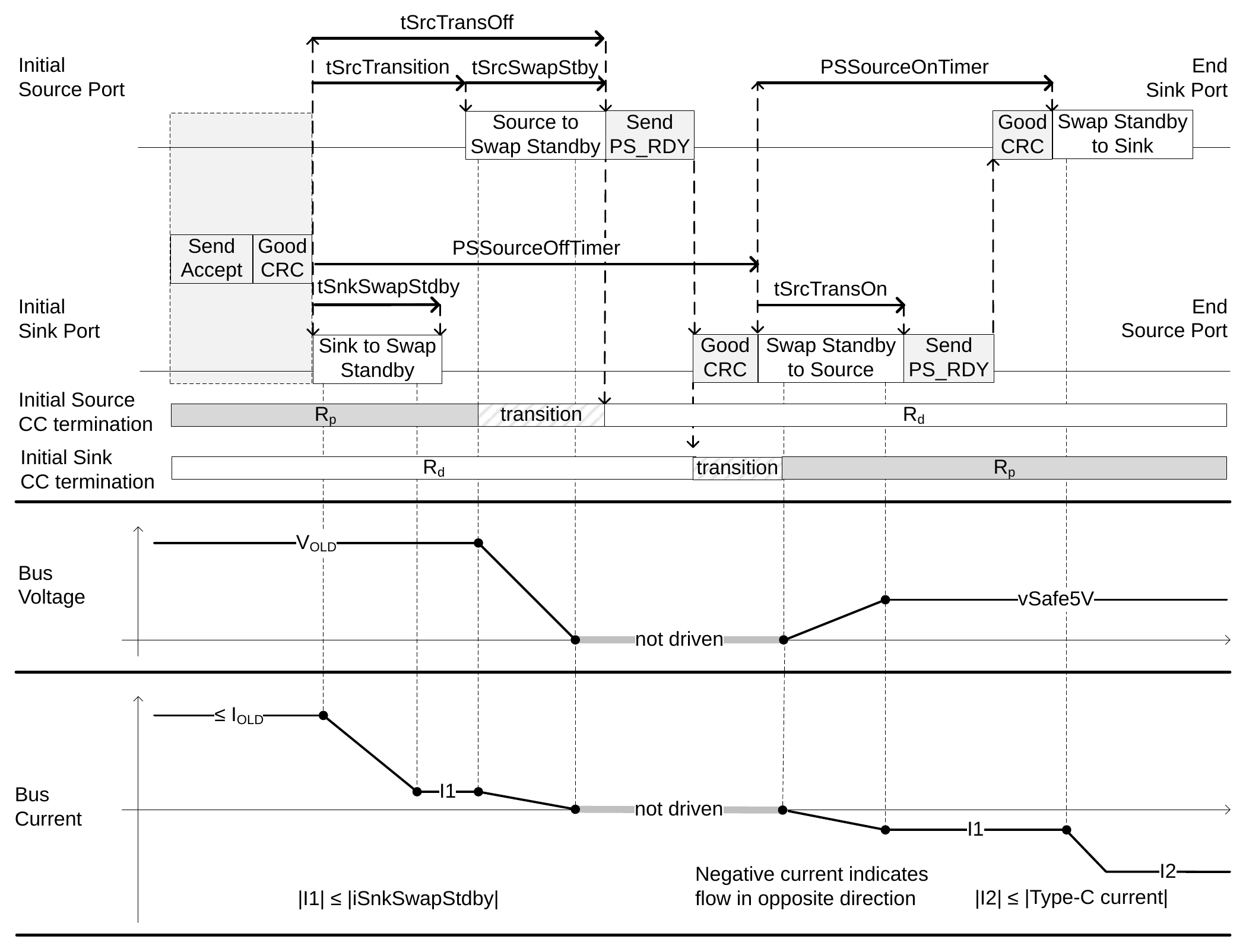
4.3.3. Power Role Swap Sequence
In Figure 4.13, a PR_Swap Message has been sent by either the Sink or the Source. See Chapter 10 for a Fast Role Swap (FRS) Sequence.
The Power Role Swap will follow the same sequence irrespective of which Port partner makes the Request:
- Once the Port Partner accepts the Request, and a GoodCRC Message is sent in return, the PSSourceOff Timer is started.
- The Sink has tSnkStdby to reduce the current consumption to iSnkSwapStdby.
- Once tSrcTransition elapses, the Source has tSrcSwapStdby to discharge VBUS.
- The Initial Source Shall transition the termination from Rp to Rd before sending PS_RDY Message.
- After the Initial Source sends a PS_RDY Message it initiates the PSSourceOn Timer.
- The New Source has tSrcTransOn to turn on VBUS and transition to vSafe5V. During this time the New Sink Shall limit its current to iSnkSwapStdby.
- Once the PS_RDY Message is sent by the New Source, the Sink can start taking the Type-C Current defined by Rp. New Contract negotiations can now take place.
Figure 4.13. Transition Diagram for a Power Role Swap
4.4. Response to Hard Resets
Hard Reset Signaling indicates a communication failure has occurred. The Source is subject to the following requirements:
- Shall drive VBUS to vSafe0V.
- These actions start tPSHardReset after the last bit of the Hard Reset Signaling has been received from the Sink or sent by the Source. The Source Shall take into consideration that the Sink May have cSnkBulkPd present until VBUS drops below vSafe0V.
- The Source Shall meet both tSafe5V and tSafe0V relative to the start of the voltage transition.
- After establishing the vSafe0V voltage condition on VBUS, the Source Shall wait tSrcRecover before re- applying VCONN and restoring VBUS to vSafe5V.
The Port Partner that drives VCONN is subject to the following requirements:
- Shall stop driving VCONN.
- If the Source was driving VCONN, then Rp Shall be removed from the CC line.
- If the Sink was driving VCONN, Rd Shall be added to the CC line.
- VCONN will meet tVCONNDischarge relative to the start of the voltage transition as shown in Figure 4.14 due to the discharge circuitry in the CablePlug. VCONN Shall meet tVCONNOn relative to VBUS reaching vSafe5V.
- tVCONNOn and tVCONNDischarge are defined in [USB-C].
Figure 4.14. Source VBUS and VCONN Response to Hard Reset
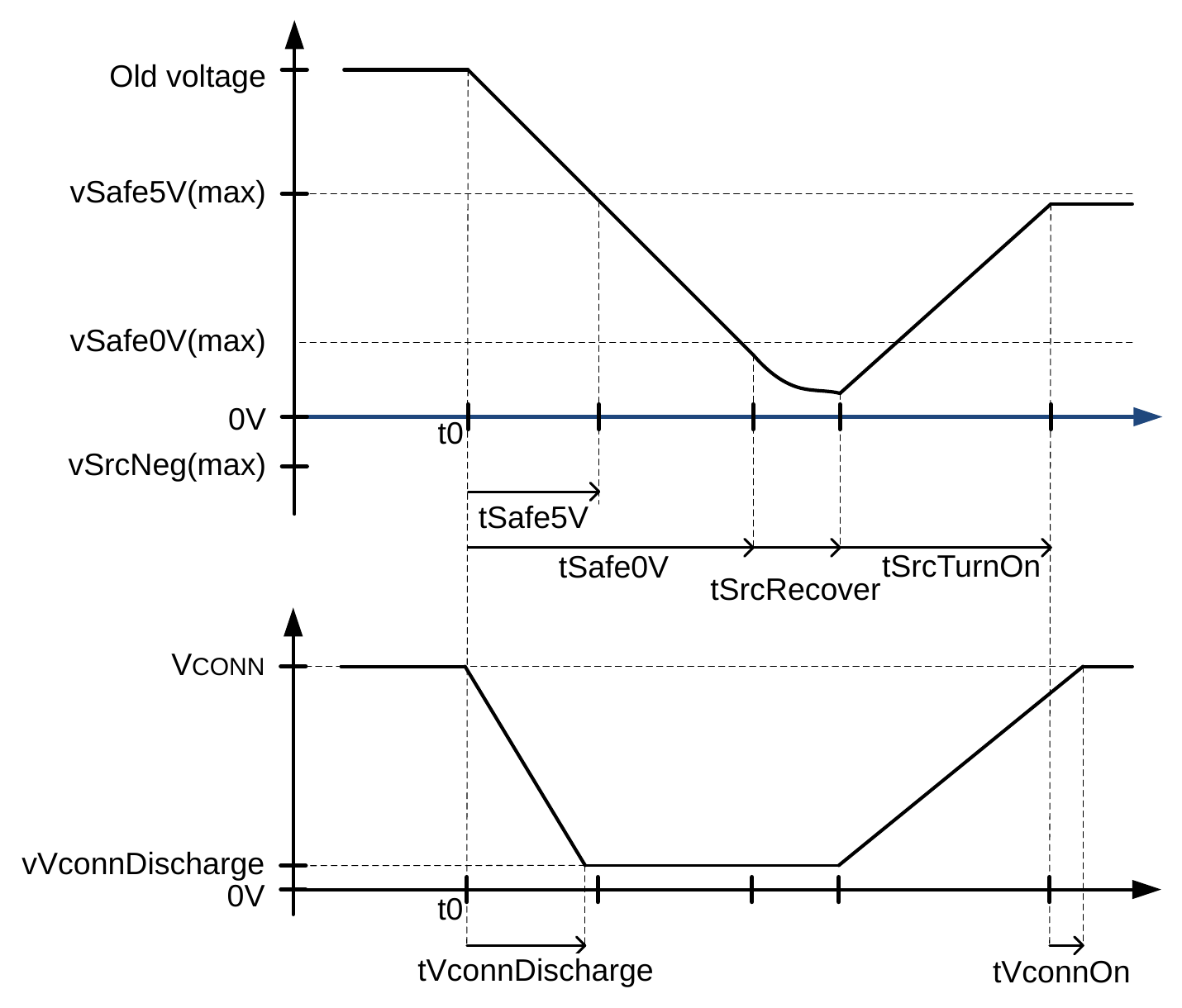
The USB connection May reset during a Hard Reset since the VBUS voltage will be less than vSafe5V for an extended period of time.
Device operation during and after a Hard Reset is defined as follows:
- Self-powered devices Should Not disconnect from USB during a Hard Reset.
- Self-powered devices operating at more than vSafe5V May Not maintain full functionality after a Hard Reset.
- Bus powered devices will disconnect from USB during a Hard Reset due to the loss of their power Source.
4.4.1. Hard Reset Sequence
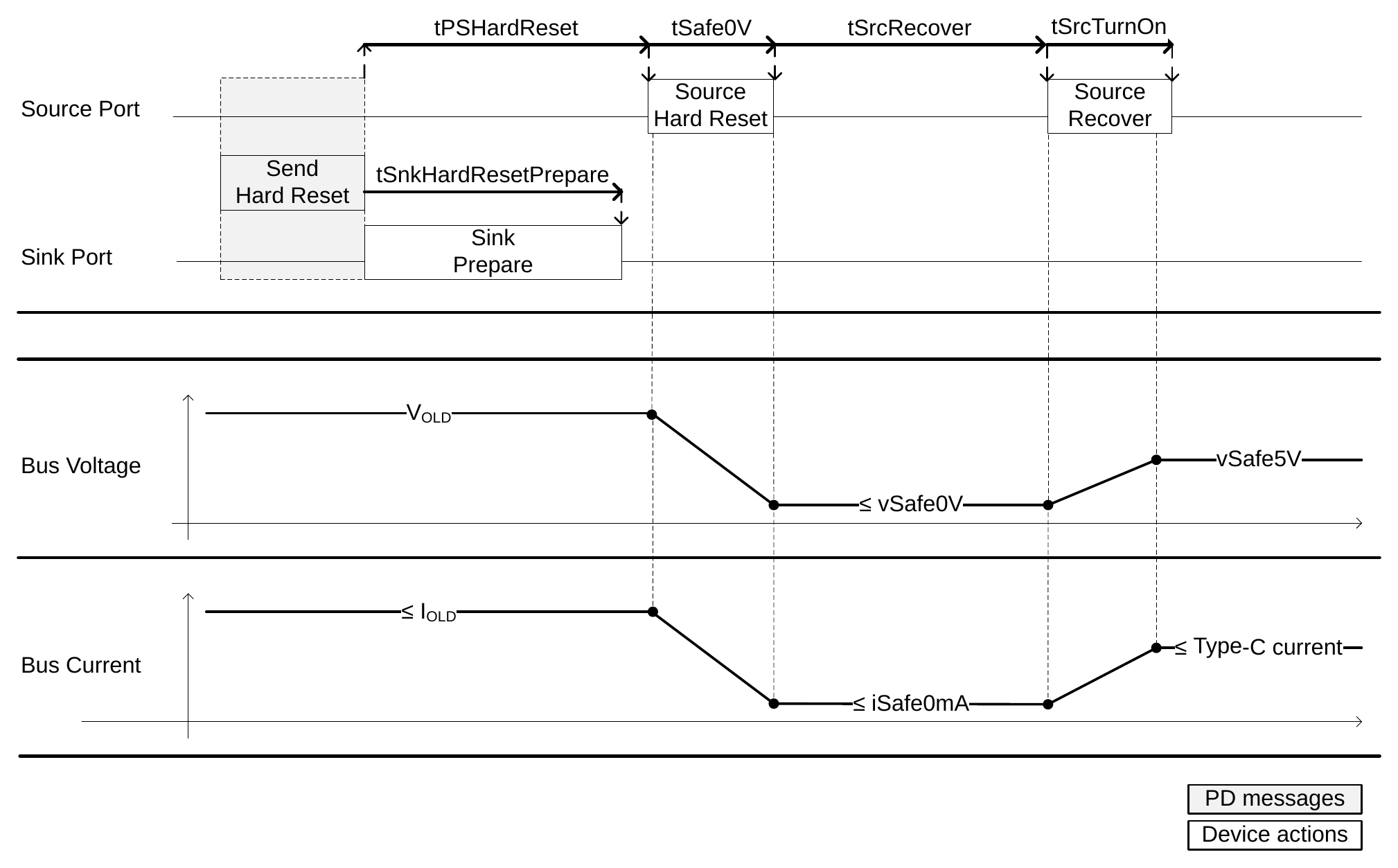
The Hard Reset transition diagram is shown in. The sequence is the same irrespective of which Port Partner started it.
- Once the Hard Reset is initiated tPSHardReset starts. The Sink has tSnkHardResetPrepare, where the current Contract is still guaranteed.
- Once tPSHardReset elapses, the Source has tSafe0V to drive the VBUS voltage to vSafe0V or lower. At this point the Sink Shall Not draw more than iSafe0mA.
- After tSrcRecover the Source applies power to VBUS. The transition to vSafe5V Shall occur within tSrc- TurnOn, and initially the current will be limited to Type-C Current until a new explicit Contract is established.
Figure 4.15. Transition diagram for a Hard Reset
4.5. Transitions
The following sections illustrate the power supply's response to common Negotiation events, including transitions initiated by a Request Message, as well as Power Role Swaps and Hard Reset scenarios.
4.5.1. Fixed and AVS transitions
The examples of PDO or APDO changes below illustrate the most common voltage and current transition requests. In all the following examples, the Sink has previously sent a Request Message to the Source. The figures group the common cases; each title states the applicable voltage/current change. These examples illustrate typical successful transitions but are not to scale.
The timing parameters that Shall be followed are listed in Table 4.6, Table 4.7, and Table 4.8.
4.5.1.1. Large-step voltage increases (Fixed or AVS)
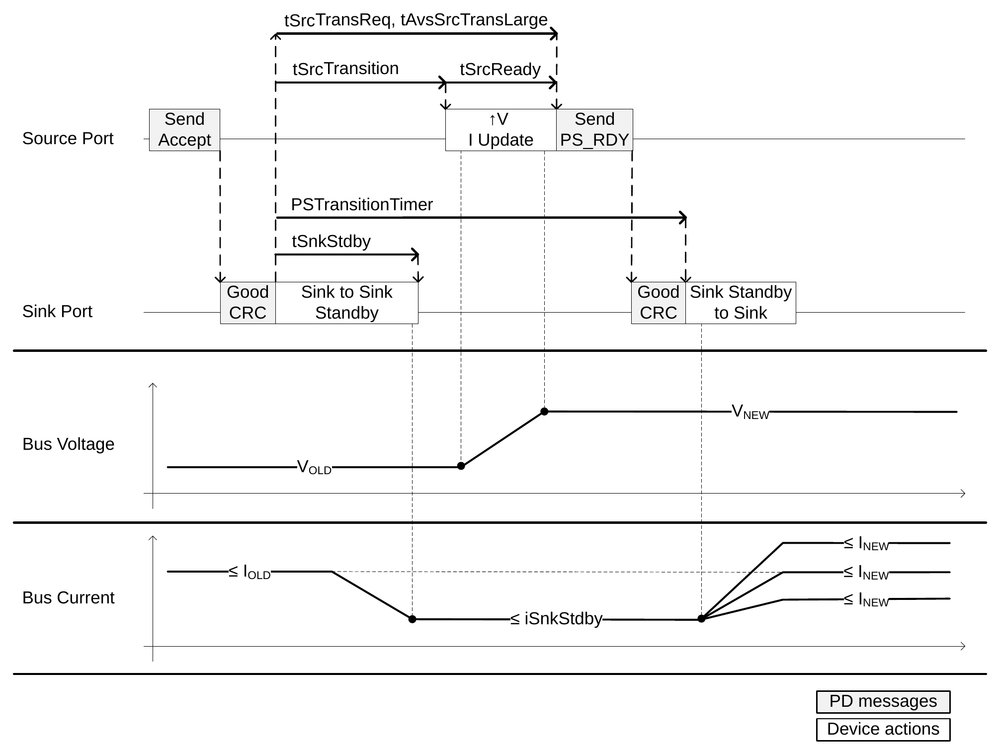
This diagram applies to fixed voltage transitions and AVS transitions where the voltage is increasing and the voltage change > vSmallStep. In these cases, the Sink Shall reduce the VBUS current to iSnkStdby as specified below.
The sequence for these types of transitions is as follows:
- The Source Policy Engine sends an Accept Message.
- The PSTransitionTimer starts immediately after the Sink completes sending the GoodCRC Message.
- tSrcTransition, tSnkStdby, and tSrcTransReq / tAvsSrcTransLarge also start at this point.
- The Sink Should reduce the current to no more than iSnkStdby within tSnkStdby. It Shall be reduced to iSnkStdby before the end of the minimum value of tSrcTransition expires.
- Once tSrcTransition elapses, the Source May start increasing the voltage. It Shall reach vNew and begin
sending a PS_RDY Message before:
- tSrcTransReq expires for transitions to a PDO.
- tAvsSrcTransLarge expires for transitions to an AVS APDO.
- The Sink acknowledges the PS_RDY Message with a GoodCRC Message and May increase its current up to the newly Negotiated value at any time, provided the required slew rate is not exceeded.
Figure 4.16. Transition Diagram for Large-step voltage increase (Fixed or AVS > vSmallStep)
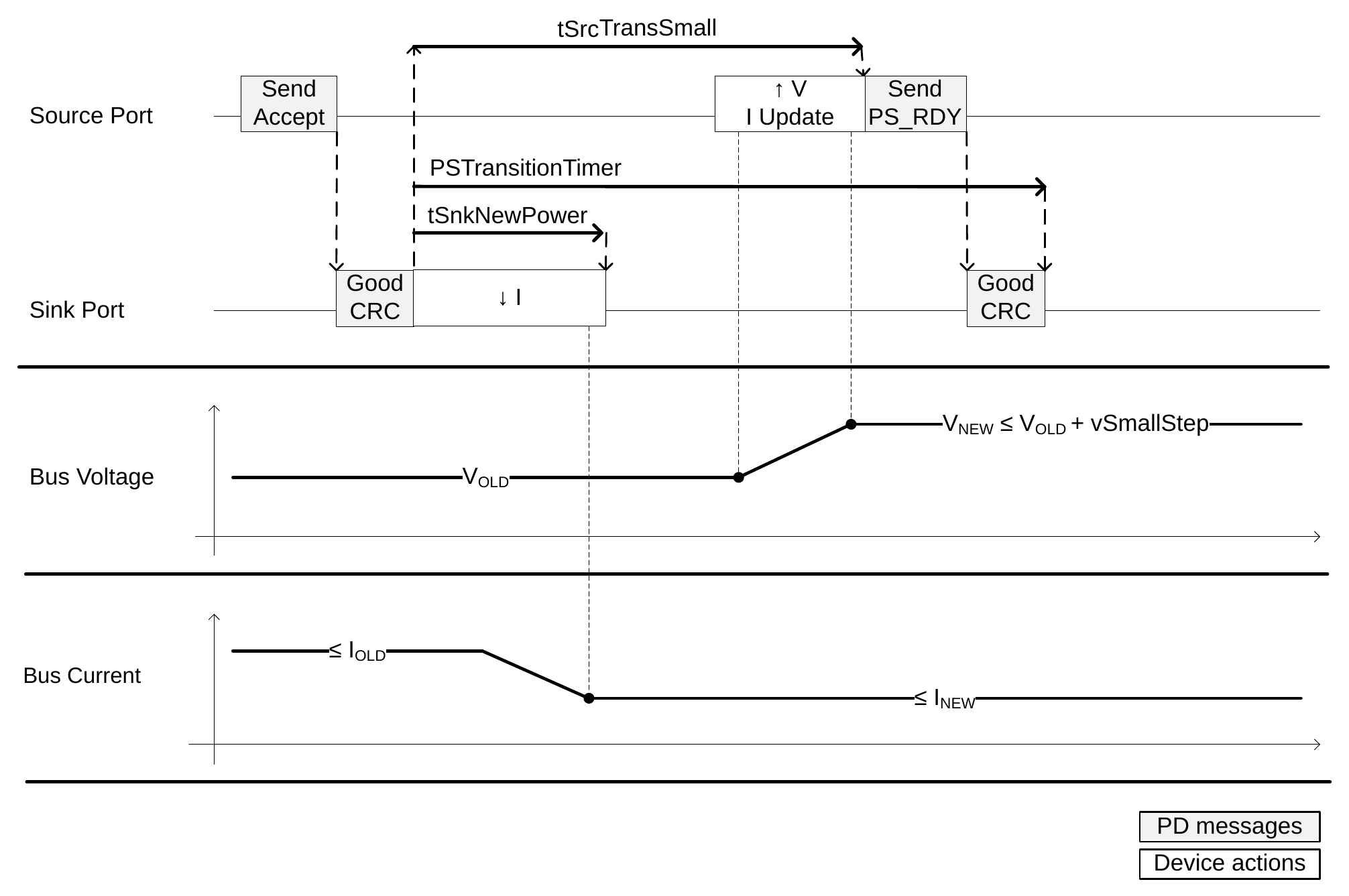
4.5.1.2. Small-step voltage increases (AVS)
Figure 4.17 applies to AVS transitions where the voltage is increasing and the voltage change ≤ vSmallStep. In these cases, the Sink can maintain the maximum current through the transition.
The sequence for these types of transitions is as follows:
- The Source Policy Engine sends an Accept Message.
- The PSTransitionTimer starts immediately after the Sink completes sending the GoodCRC Message.
- There is no requirement for the Sink to reduce the current during the transition period.
- The Source May immediately start increasing the voltage. It Shall reach vNew and send a PS_RDY Message before tSrcTransSmall expires.
- The Sink acknowledges the PS_RDY Message with a GoodCRC Message and May increase its current up to the newly Negotiated value at any time, provided the required slew rate is not exceeded.
Figure 4.17. Transition Diagram for Small-step voltage increase (AVS ≤ vSmallStep), current unchanged or increased
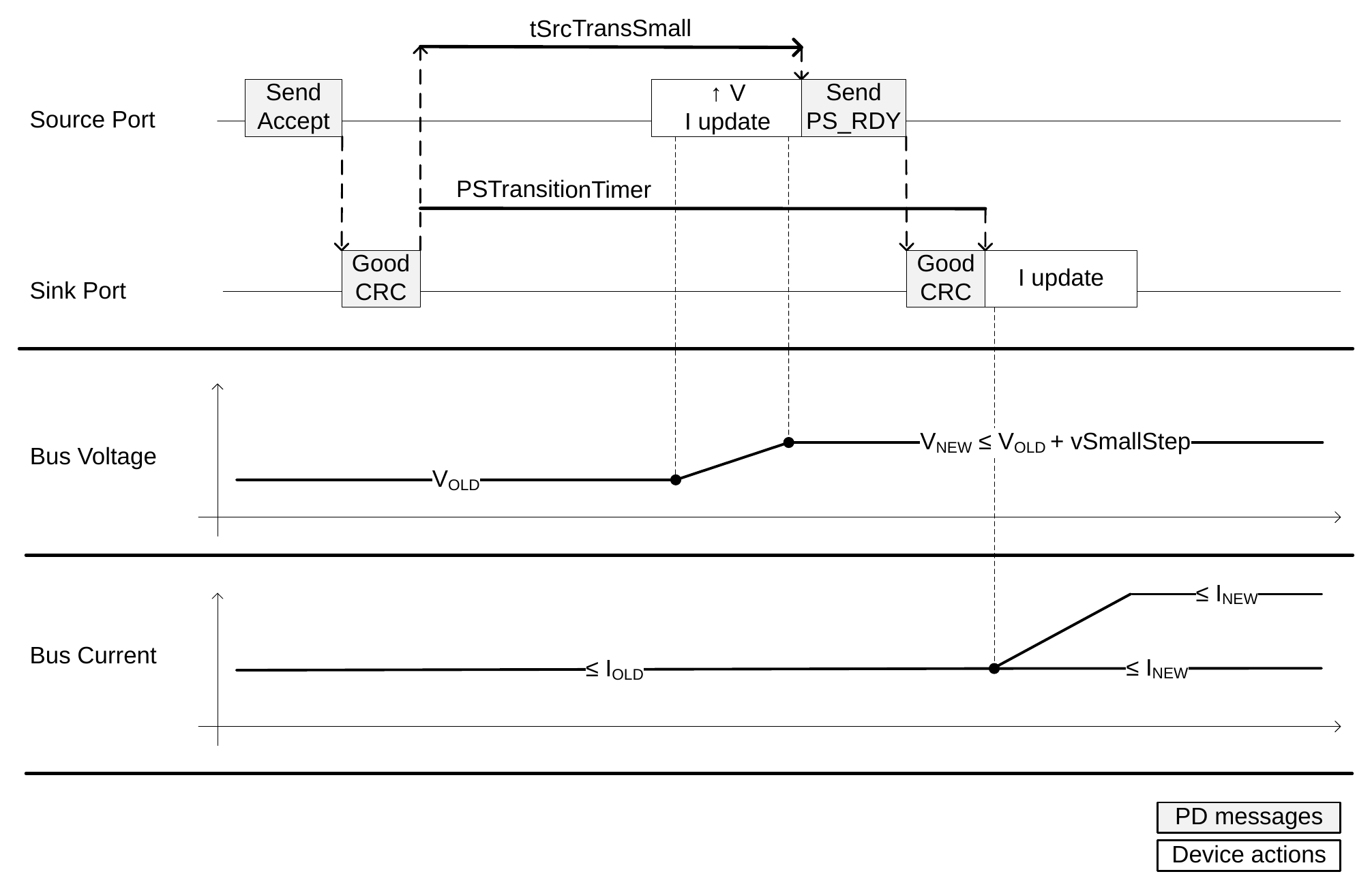
Figure 4.18 applies to AVS transitions where the voltage is increasing and the voltage change ≤ vSmallStep with a decrease in current.
The sequence for these types of transitions is as follows:
- The Source Policy Engine sends an Accept Message.
- The
PSTransitionTimerstarts immediately after the Sink completes sending the GoodCRC Message. - The Sink has
tSnkNewPowerto reduce the VBUS current to a maximum ofI_{NEW}. - The Source Shall reach
vNewand send aPS_RDYMessage beforetSrcTransSmallexpires. - The Source Shall wait
tSnkNewPowerbefore changing any current limit protection related toI_{NEW}. - The Sink acknowledges the
PS_RDYMessage with a GoodCRC Message.
Figure 4.18. Transition Diagram for Small-step voltage increase (AVS ≤ vSmallStep), current decreased
4.5.1.3. Unchanged or decreased voltage transitions (current unchanged, increased, or decreased)
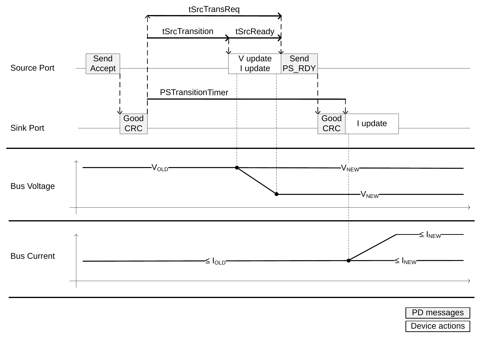
The process for these transitions depends on whether the voltage is unchanged or decreased, and whether the current is increased, decreased, or unchanged.
- The Source Policy Engine sends an Accept Message.
- The
PSTransitionTimerstarts immediately after the Sink completes sending the GoodCRC Message. - There is no requirement for the Sink to reduce the current during the transition period.
- The Source Shall wait
tSrcTransitionbefore starting to decrease the voltage or updating any current protection thresholds as needed. - Once
tSrcTransitionelapses, the Source May start decreasing the voltage. It Shall reachvNewand begin sending aPS_RDYMessage before:tSrcTransReqexpires for transitions to a PDO.tAvsSrcTransLargeexpires for transition to an AVS APDO and the voltage change is >vSmallStep.
- The Sink acknowledges the
PS_RDYMessage with a GoodCRC Message and May increase its current up to the newly Negotiated value at any time, as long as the required slew rate is not exceeded.
Figure 4.19. Transition Diagram for voltage unchanged or decreased with current unchanged or increased
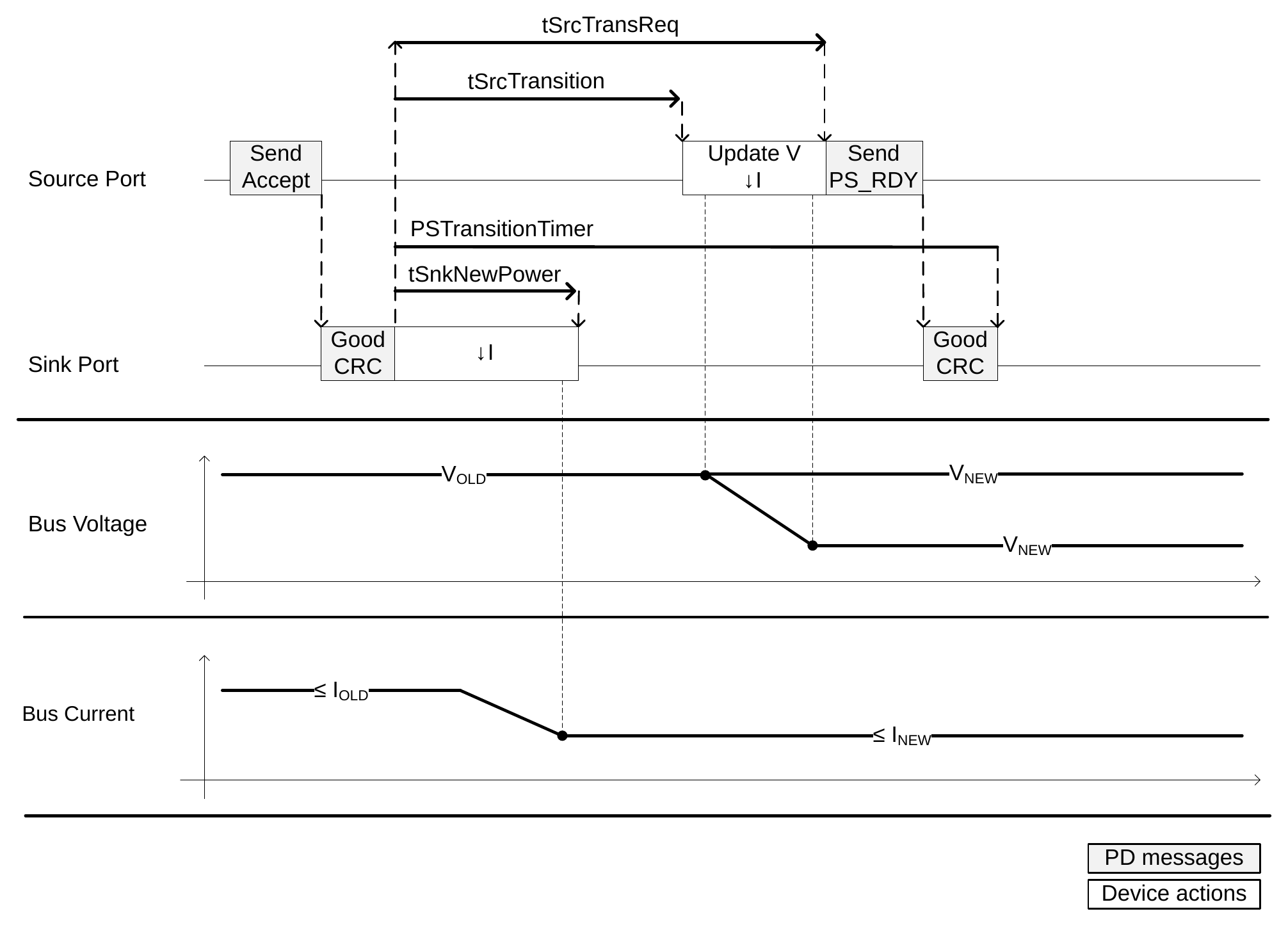
If the current needs to be decreased, the previous sequence shall be followed with one difference as shown in Figure 4.20:
- The Sink Should reduce the current to a value that is less than or equal to the newly Negotiated value (
I_{NEW}) withintSnkNewPower. It Shall reachI_{NEW}before the minimum value oftSrcTransitionexpires.
Figure 4.20. Transition Diagram for voltage unchanged or decreased with current decreased
4.5.2. PPS voltage or current changes
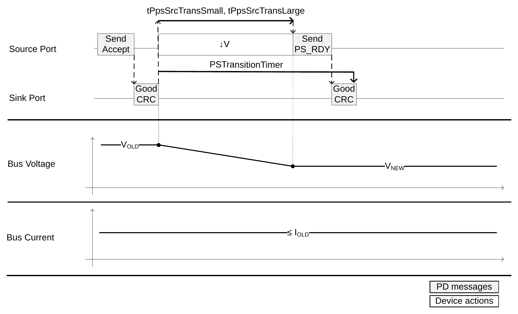
4.5.2.1. PPS voltage transitions (CV Mode)
This sequence is valid for any PPS voltage transition (while in CV Mode), and any small AVS transition that is vAvsSmallStep or smaller.
Compared with transitions that use fixed voltage contracts, the process of starting the voltage transition can begin immediately after the Sink acknowledges the Accept Message with a GoodCRC Message. Additionally, the Sink can operate at any current level, up to the maximum value defined by the Contract. Figure 4.21 shows the sequence when the voltage is increased and Figure 4.22 shows the sequence when it is decreased.
Figure 4.21. Transition Diagram for PPS voltage increase (CV Mode)
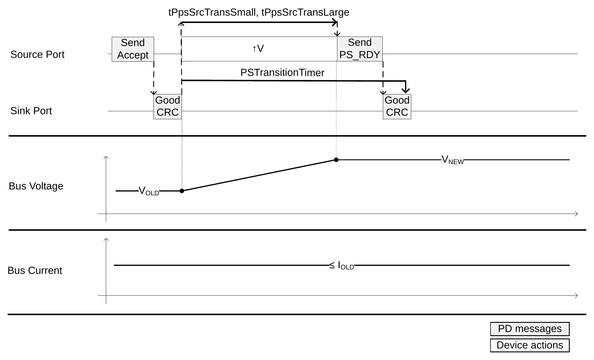
Figure 4.22. Transition Diagram for PPS voltage decrease (CV Mode)
4.5.2.2. PPS current transitions (CL Mode)
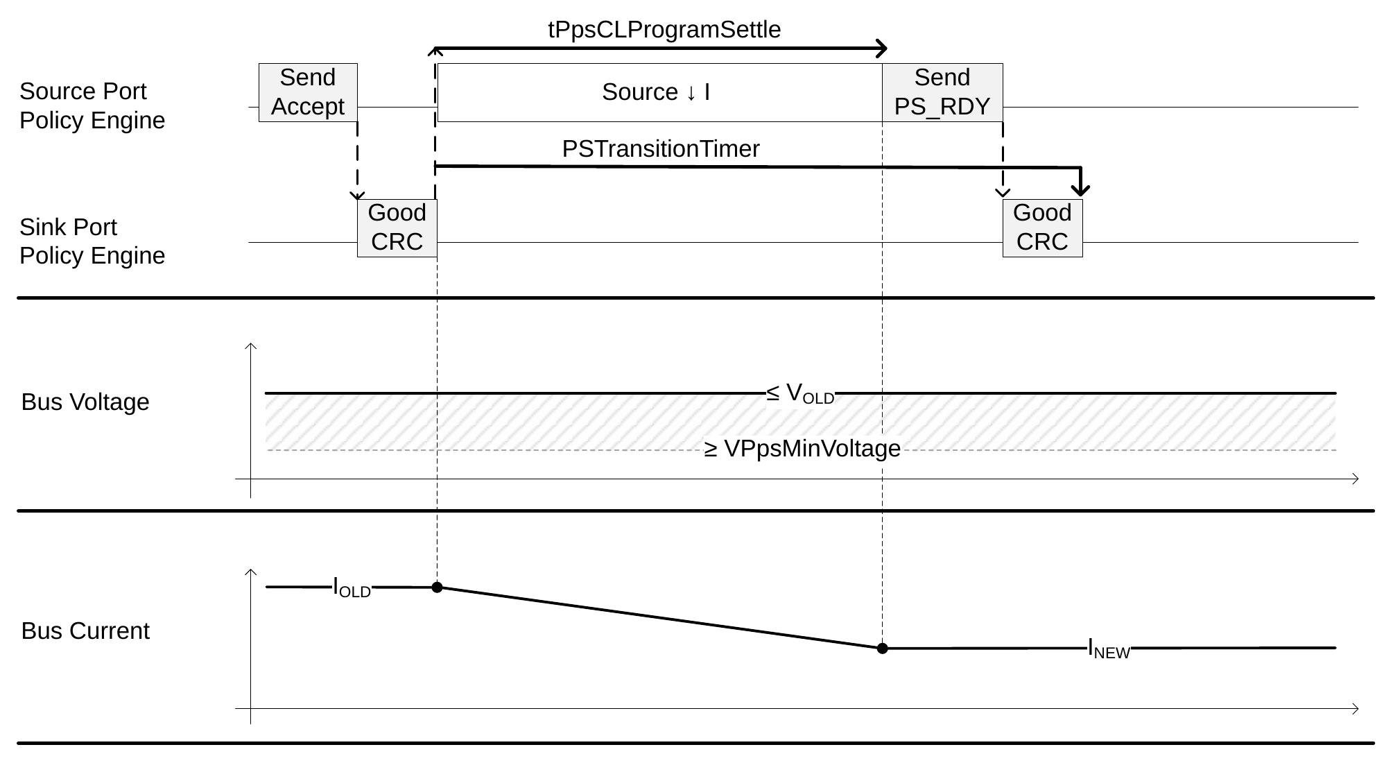
In PPS, the Sink can Request a change in current while operating in Current Limit (CL) Mode. In this scenario, the Source is controlling the VBUS current instead of the VBUS voltage. The VBUS voltage can take any value between vPpsMinVoltage, and the Output Voltage value used in the PPS Request Data Object. Figure 4.23 shows the transition for changing current in PPS.
Figure 4.23. Transition Diagram for PPS current increase (CL Mode)
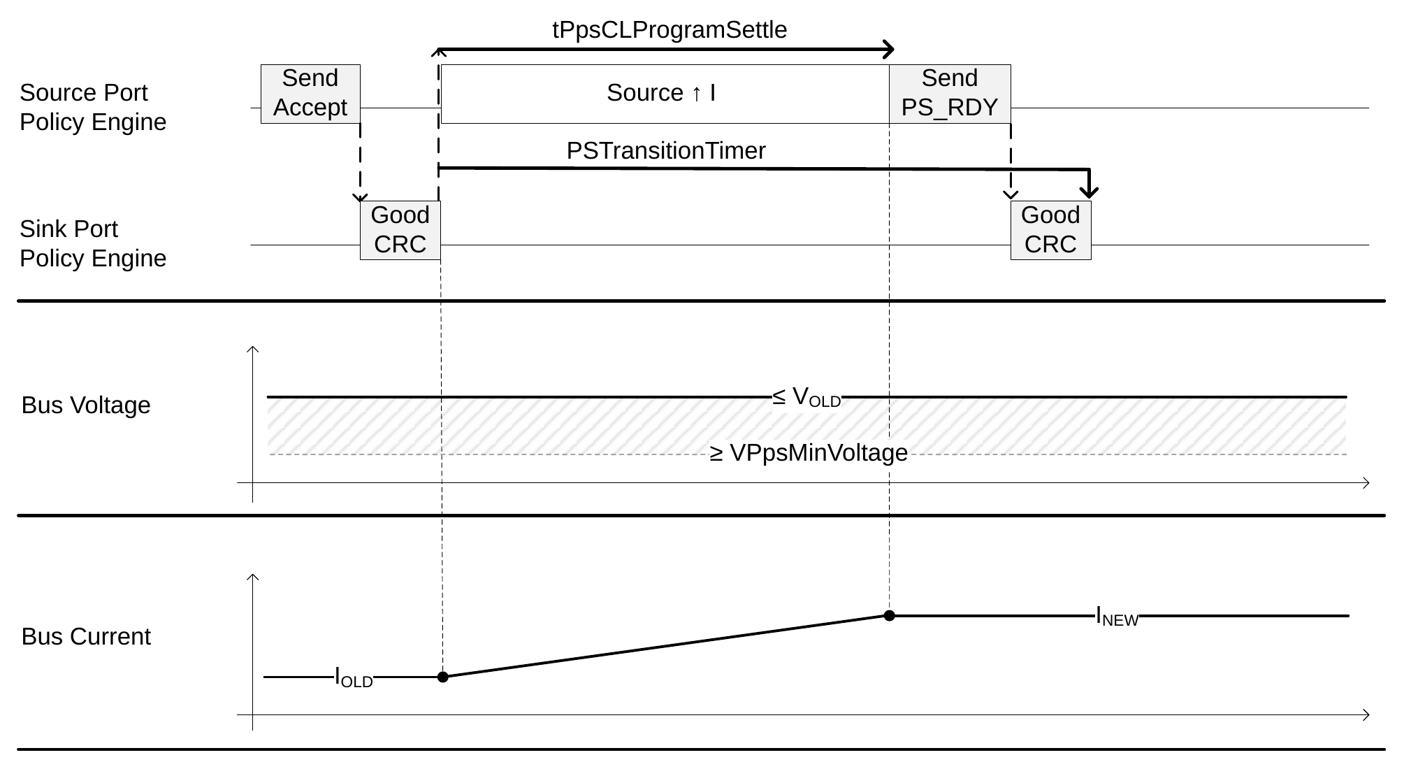
Figure 4.24. Transition Diagram for PPS current decrease (CL Mode)
4.6. VCONN Power Cycle
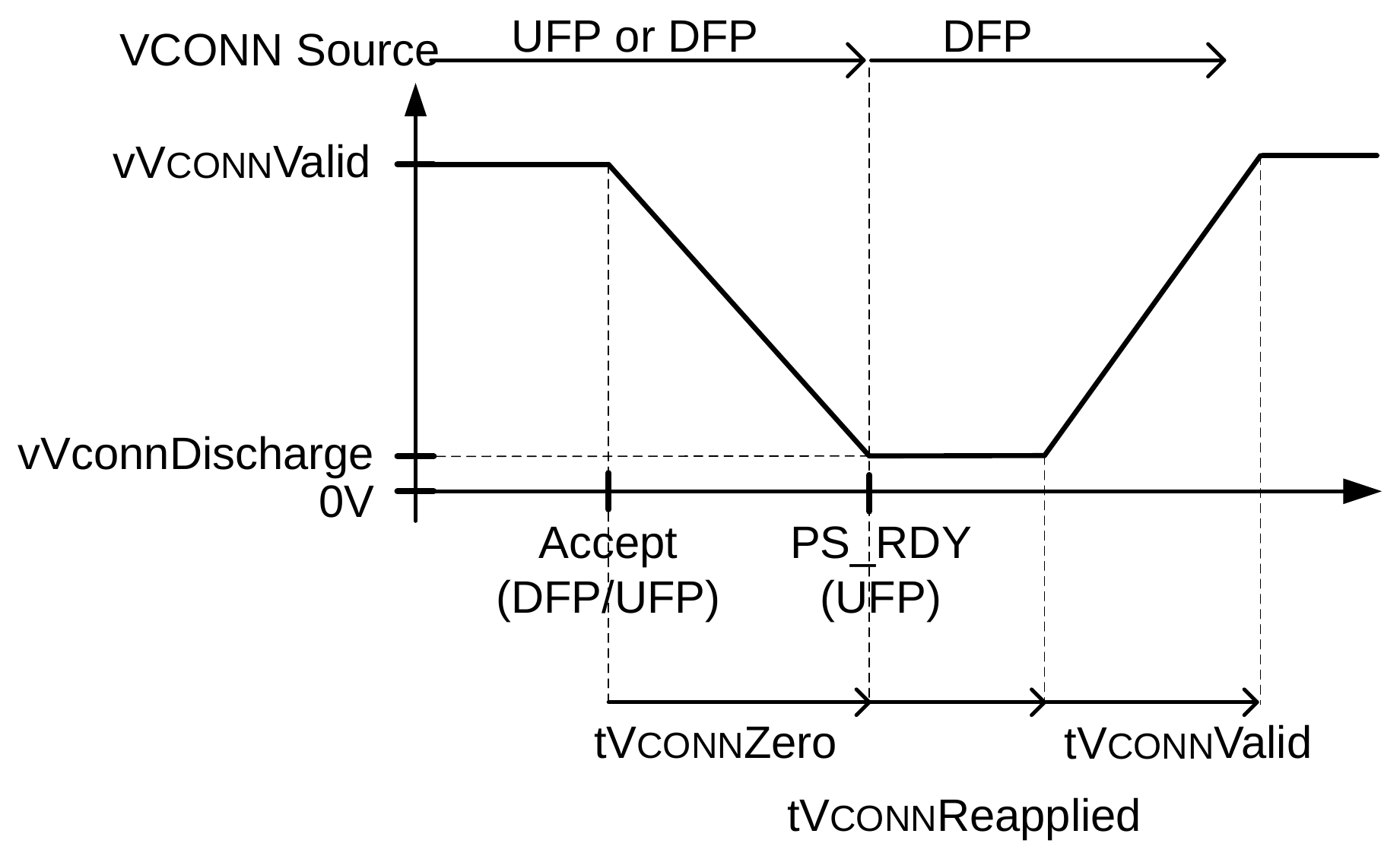
When performing a VCONN Power Cycle during a Data Reset, the following steps Shall be followed:
- Following the last bit of the GoodCRC Message acknowledging the Accept Message, the initial VCONN Source Shall turn off VCONN and ensure it is below [USB-C]
vRaReconnectwithintVCONNZero. - When VCONN is below
vRaReconnect, the initial VCONN Source Shall send aPS_RDYMessage. Note: for a Data Reset requested by the UFP, if the UFP was not sourcing VCONN, it Shall send thePS_RDYMessage. - The new VCONN Source Shall wait
tVCONNReappliedfollowing the last bit of the GoodCRC Message acknowledging thePS_RDYMessage before sourcing VCONN. The new VCONN Shall ensure VCONN is withinvVCONNValid(see [USB-C]) withintVCONNValid.
Figure 4.25 illustrates the VCONN Power Cycle process.
Figure 4.25. Data Reset VCONN Power Cycle
4.7. Electrical Parameters
4.7.1. Source Electrical Parameters
The Source Electrical Parameters that Shall be followed are specified in Table 4.6.
Table 4.6. Source Electrical Parameters
| Parameter Name | Min Value | Nom Value | Max Value | Unit | Description | |
|---|---|---|---|---|---|---|
cSrcBulk |
10 | µF | Source bulk capacitance when a Port is powered from a dedicated supply. | |||
cSrcBulkShared |
120 | µF | Source bulk capacitance when a Port is powered from a shared supply.[^1] | |||
DNL |
-1 | 0 | +1 | LSB | Differential Non-Linearity Deviation between ideal analog values corresponding to adjacent input digital values | |
iPpsCLMin |
1 | A | PPS Minimum Current Limit setting. | |||
iPpsCLNew |
≤ 3A | -150 | 150 | mA | Current Limit Accuracy 1A ≤ Operating Current ≤ 3A | |
iPpsCLNew |
> 3A | -5 | 5 | % | Current Limit Accuracy Operating current > 3A | |
iPpsCLStep |
50 | mA | PPS Current Limit programming step size (1 LSB). | |||
iPpsCLLoadReleaseRate |
-150 | mA/µs | Maximum load decrease slew rate during Current Limit setpoint changes. | |||
iPpsCLLoadStepRate |
150 | mA/µs | Maximum load increase slew rate during Current Limit setpoint changes. | |||
iPpsCLTransient |
Load increase | New load + 100 | mA | Allowed output current overshoot when a load increase occurs while in CL Mode. | ||
iPpsCLTransient |
Load decrease | New load – 100 | mA | Allowed output current undershoot when a load decrease occurs while in CL Mode. | ||
iPpsCVCLTransient |
iPpsCLNew - 100 |
New load + 500 | mA | CV to CL transient current bounds. See Section 4.1.3.2.2. | ||
tAvsTransient |
5 | ms | The maximum time for the AVS to be between vAvsNew and vAvsValid in response to a load transient. |
|||
tAvsSrcTransLarge |
0 | 700 | ms | The time the AVS set-point Shall transition between requested voltages for steps larger than vAvsSmallStep. |
||
tAvsSrcTransSmall |
0 | 50 | ms | The time the AVS set-point Shall transition between requested voltages for steps smaller than vAvsSmallStep. |
||
tNewSnk |
15 | ms | Time allowed for an Initial Source in Swap Standby to transition to New Sink operation. | |||
tPpsCLCVTransient |
275 | ms | CL to CV transient voltage settling time. | |||
tPpsCLProgramSettle |
250 | ms | PPS Current Limit programming settling time. |
| Parameter Name | Min Value | Nom Value | Max Value | Unit | Description | |
|---|---|---|---|---|---|---|
| tPpsCLSettle | 250 | ms | CL load transient current settling time. | |||
| tPpsCVCLTransient | 250 | ms | CV to CL transient settling time. | |||
| tPpsSrcTransLarge | 0 | 275 | ms | The time the Programmable Power Supply's set-point Shall transition between requested voltages for steps larger than vPpsSmallStep. | ||
| tPpsSrcTransSmall | 0 | 25 | ms | The time the Programmable Power Supply's set-point Shall transition between requested voltages for steps less than or equal to vPpsSmallStep. | ||
| tPpsTransient | Target load ≥ 60mA | 5 | ms | The maximum time for the Programmable Power Supply to be between vPpsNew and vPpsValid in response to a load transient when target load is greater than or equal to 60mA. | ||
| tPpsTransient | Target load < 60mA | 150 | ms | The maximum time for the Programmable Power Supply to be between vPpsNew and vPpsValid in response to a load transient when target load is less than 60mA. | ||
| tSrcReady | SPR Mode | 285 | ms | Time from positive/negative transition start (t0) to when the Source is ready to provide the newly Negotiated power level. Applies only to SPR Mode voltage transitions. | ||
| tSrcReady | EPR Mode | 720 | ms | Time from positive/negative transition start (t0) to when the Source is ready to provide the newly Negotiated power level. Applies to EPR Mode voltage transitions and any voltage transition that either begins or ends in EPR Mode. | ||
| tSrcRecover | SPR Mode | 0.66 | 1.0 | s | Time allotted for the Source to recover. | |
| tSrcRecover | EPR Mode | 1.085 | 1.425 | s | Time allotted for the Source to recover. | |
| tSrcSettle | SPR Mode | 275 | ms | Time from positive/negative transition start (t0) to when the transitioning voltage is within the range vSrcNew. Applies only to SPR Mode voltage transitions. | ||
| tSrcSettle | EPR Mode | 700 | ms | Time from positive/negative transition start (t0) to when the transitioning voltage is within the range vAvsNew. Applies to EPR Mode voltage transitions and any voltage transition that either begins or ends in EPR Mode. | ||
| tSrcSwapStdby | 650 | ms | The maximum time for the Source to transition to Swap Standby. |
| Parameter Name | Min Value | Nom Value | Max Value | Unit | Description | |
|---|---|---|---|---|---|---|
| tSrcTransient | 5 | ms | The maximum time for the Source output voltage to be between vSrcNew and vSrcValid in response to a load transient when target load is greater than or equal to 60mA. | |||
| tSrcTransient | 150 | ms | The maximum time for the Source output voltage to be between vSrcNew and vSrcValid in response to a load transient when target load is less than 60mA. | |||
| tSrcTransition | 25 | 35 | ms | The time the Source Shall wait before transitioning the power supply to ensure that the Sink has sufficient time to prepare (does not apply to transitions within the same PPS or AVS APDO). | ||
| tSrcTransOff | 690 | ms | Time from the last bit of the GoodCRC Message acknowledging the Accept Message in response to the PR_Swap Message until the PS_RDY Message must be started. Applies only to SPR Mode voltage transitions. | |||
| tSrcTransOn | 280 | ms | Time from the last bit of the GoodCRC Message acknowledging the PS_RDY Message sent by the New Source, in response to the PR_Swap Message until the PS_RDY Message must be started. | |||
| tSrcTransReq | SPR Mode | 325 | ms | Time from the last bit of the GoodCRC Message acknowledging the Accept Message in response to the Request Message until the PS_RDY Message must be started. Applies only to SPR Mode voltage transitions. | ||
| tSrcTransReq | EPR Mode | 760 | ms | Time from the last bit of the GoodCRC Message acknowledging the Accept Message in response to the Request Message until the PS_RDY Message must be started. Applies to EPR Mode voltage transitions and any voltage transition that either begins or ends in EPR Mode. | ||
| tSrcTurnOn | 275 | ms | Transition time from vSafe0V to vSafe5V. | |||
| tReducePowerAlert | 2000 | 2400 | ms | Time between an alert and the New Source Capabilities when reducing Port Present PDP. | ||
| tDpsColdStart | 15 | minute | Time for a DPS Source to maintain Port Present PDP = Port Maximum PDP after a cold start before thermal limiting. | |||
| tDpsRegular | 1 | minute | Time between New Source Capabilities for a DPS Source due to thermal limiting. |
| Parameter Name | Min Value | Nom Value | Max Value | Unit | Description | |
|---|---|---|---|---|---|---|
| vAvsMaxVoltage | APDO Max Voltage×0.95 | APDO Max Voltage×1.05 | V | Maximum Voltage Field in the AVS APDO. | ||
| vAvsMinVoltage | APDO Min Voltage×0.95 | APDO Min Voltage×1.05 | V | Minimum Voltage Field in the AVS APDO. | ||
| vAvsNew | RDO Output Voltage×0.95 | RDO Output Voltage | RDO Output Voltage×1.05 | V | Adjustable RDO Output Voltage measured at the Source receptacle. | |
| vAvsSlewNeg | -30 | mV/µs | AVS maximum slew rate for negative voltage changes. | |||
| vAvsSlewPos | 30 | mV/µs | AVS maximum slew rate for positive voltage changes. | |||
| vAvsSmallStep | -1.0 | 1.0 | V | AVS step size defined as a small step relative to the previous vAvsNew. | ||
| vAvsStep | 100 | mV | AVS voltage programming step size. | |||
| vAvsValid | -0.5 | 0.5 | V | The range in addition to vAvsNew which the AVS output is considered Valid during and after a transition as well as in response to a transient load condition. | ||
| vPpsCLCVTransient | Operating Voltage×0.95 – 0.1V | Operating Voltage×1.05 + 0.1V | V | CL to CV load transient voltage bounds. | ||
| vPpsMaxVoltage | APDO Max Voltage×0.95 | APDO Max Voltage×1.05 | V | Maximum Voltage Field in the Programmable Power Supply APDO. | ||
| vPpsMinVoltage | APDO Min Voltage×0.95 | APDO Min Voltage×1.05 | V | Minimum Voltage Field in the Programmable Power Supply APDO. | ||
| vPpsNew | RDO Output Voltage×0.95 | RDO Output Voltage | RDO Output Voltage×1.05 | V | Programmable RDO Output Voltage measured at the Source receptacle. | |
| vPpsShutdown | APDO Minimum Voltage×0.85 | APDO Minimum Voltage×0.95 | V | The voltage at which the PPS shuts down when operating in CL. | ||
| vPpsSlewNeg | -30 | mV/µs | Programmable Power Supply maximum slew rate for negative voltage changes | |||
| vPpsSlewPos | 30 | mV/µs | Programmable Power Supply maximum slew rate for positive voltage changes | |||
| vPpsSmallStep | -500 | 500 | mV | PPS Step size defined as a small step relative to the previous vPpsNew. | ||
| vPpsStep | 20 | mV | PPS voltage programming step size (1 LSB). | |||
| vPpsValid | -0.1 | 0.1 | V | The range in addition to vPpsNew which the Programmable Power Supply output is considered Valid in response to a load step. | ||
| vSrcNeg | -0.3 | V | Most negative voltage allowed during transition. | |||
| vSrcNew | Fixed Supply | PDO Voltage×0.95 | PDO Voltage | PDO Voltage×1.05 | V | Fixed Supply output measured at the Source receptacle. |
| Parameter Name | Min Value | Nom Value | Max Value | Unit | Description | |
|---|---|---|---|---|---|---|
| vSrcNew | Variable Supply | PDO Minimum Voltage | PDO Maximum Voltage | V | Variable Supply output measured at the Source receptacle. | |
| vSrcNew | Battery Supply | PDO Minimum Voltage | PDO Maximum Voltage | V | Battery Supply output measured at the Source receptacle. | |
| vSrcPeak | PDO Voltage×0.90 | PDO Voltage×1.05 | V | The range that a Fixed Supply or EPR AVS in Peak Current operation is allowed when overload conditions occur. | ||
| vSrcSlewNeg | -30 | mV/µs | Maximum slew rate allowed for negative voltage transitions. Limits current based on a 3 A connector rating and maximum Sink bulk capacitance of 100 µF. | |||
| vSrcSlewPos | 30 | mV/µs | Maximum slew rate allowed for positive voltage transitions. Limits current based on a 3 A connector rating and maximum Sink bulk capacitance of 100 µF. | |||
| vSrcValid | -0.5 | 0.5 | V | The range in addition to vSrcNew which a newly Negotiated voltage is considered Valid during and after a transition as well as in response to a transient load condition. This range also applies to vSafe5V. |
4.7.2. Sink Electrical Parameters
The Sink Electrical Parameters that Shall be followed are specified in Table 4.7.
Table 4.7. Sink Electrical Parameters
| Parameter Name | Min Value | Nom Value | Max Value | Unit | Description |
|---|---|---|---|---|---|
| cSnkBulk | See [USB3] | Sink bulk capacitance on VBUS at Attach and during FRS after the Initial Source stops sourcing and prior to establishing the First Explicit Contract. | |||
| cSnkBulkPd | 100 | µF | Bulk Capacitance that a Sink is allowed to present on VBUS after a successful Negotiation. | ||
| iLoadReleaseRate | -150 | mA/ µs | Load release di/dt. | ||
| iLoadStepRate | 150 | mA/ µs | Load step di/dt. | ||
| iPpsCLLoadStep | -500 | 500 | mA | Maximum Current set-point change while operating in CL Mode. | |
| iSafe0mA | 1.0 | mA | Maximum current a Sink is allowed to draw when VBUS is driven to vSafe0V. | ||
| iSnkStdby | 500 | mA | Maximum current during voltage transition. | ||
| iSnkSwapStdby | 2.5 | mA | Maximum current a Sink can draw during Swap Standby. Ideally this current is very near to 0 mA largely influenced by Port leakage current. | ||
| pHubSusp | 125 | mW | Suspend power consumption for a Hub. 25mW + 25mW per downstream Port for up to 4 ports. | ||
| pSnkSusp | 25 | mW | Suspend power consumption for a Peripheral Device. | ||
| tNewSrc | 275 | ms | Maximum time allowed for an Initial Sink in Swap Standby to transition to New Source operation. |
| Parameter Name | Min Value | Nom Value | Max Value | Unit | Description |
|---|---|---|---|---|---|
| tSnkHardResetPrepare | 15 | ms | Time allotted for the Sink power electronics to prepare for a Hard Reset. | ||
| tSnkNewPower | 15 | ms | Maximum transition time between power levels. | ||
| tSnkRecover | 150 | ms | Time for the Sink to resume USB Default Operation. | ||
| tSnkStdby | 15 | ms | Time to transition to Sink Standby from Sink. | ||
| tSnkSwapStdby | 15 | ms | Maximum time for the Sink to transition to Swap Standby. | ||
| vSprMax | 24 | V | A Sink Should tolerate this VBUS voltage without damage. |
- If more bypass capacitance than cSnkBulk (max) or cSnkBulkPd (max) is required in the Device, then the Device Shall incorporate some form of VBUS surge current limiting as described in [USB3].
4.7.3. Common Electrical Parameters
Electrical Parameters that are common to both the Source and the Sink that Shall be followed are specified in Table 4.8.
Table 4.8. Common Source/Sink Electrical Parameters
| Parameter Name | Min Value | Nom Value | Max Value | Unit | Description |
|---|---|---|---|---|---|
| tSafe0V | 650 | ms | Time to reach vSafe0V (max). | ||
| tSafe5V | 275 | ms | Time to reach vSafe5V (max). | ||
| tVCONNReapplied | 10 | 20 | ms | When the UFP is the VCONN Source: time from the last bit of the GoodCRC Message acknowledging the PS_RDY Message until VCONN is within vVCONNValid (see [USBC]). When the DFP is the VCONN Source: time from when VCONN drops below vRaReconnect. | |
| tVCONNValid | 0 | 5 | ms | Time from tVCONNReapplied until VCONN is within vVCONNValid (see [USB-C]). | |
| tVCONNZero | 125 | ms | Time from the last bit of the GoodCRC acknowledging the Accept Message in response to the Data_Reset Message until VCONN is below vRaReconnect (see [USB-C]). | ||
| vSafe0V | 0 | 0.8 | V | Safe operating voltage at "zero volts". | |
| vSafe5V | 4.75 | 5.5 | V | Safe operating voltage at 5V. See [USB2] and [USB3] for allowable VBUS voltage range. |
- tVCONNStable (See [USB-C]) still applies.