
7.5 KiB
7.5 KiB
10. Layout
| Pin Number | Pin Name | Layout Guidelines |
|---|---|---|
| Bottom Pad 33 | GND |
Connect this ground pad to the ground plane through a low impedance path. Use at least five vias to connect to the PCB ground planes to ensure sufficient thermal dissipation directly under the IC. |
| 1 2 |
CSONCSOP |
Run two dedicated traces with sufficient width in parallel (close to each other to minimize the loop area) from the two terminals of the battery current sensing resistor to the IC. Place the differential mode and common-mode RC filter components in the general proximity of the controller. Route the current sensing traces through vias to connect the center of the pads; or route the traces into the pads from the inside of the current sensing resistor. The following drawings show the two preferred ways of routing current sensing traces. 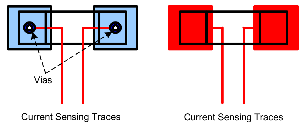 |
| 3 | VSYS |
This signal pin provides feedback for the system bus voltage. Place the optional RC filter in the general proximity of the controller. Run a dedicated trace from the system bus to the pin and do not route near the switching traces. Do not share the same trace with the signal routing to the DCIN pin OR diodes and the CSOP trace. |
| 4 | BOOT2 |
Switching pin. Place the bootstrap capacitor in the general proximity of the controller. Use sufficiently wide traces. Avoid any sensitive analog signal traces from crossing over or getting close. |
| 5 6 |
UGATE2PHASE2 |
Run these two traces in parallel fashion with sufficient width. Avoid any sensitive analog signal traces from crossing over or getting close. Route the PHASE2 trace to the high-side MOSFET source pin instead of general copper.Place the IC close to the gate terminals of the switching MOSFETs and keep the gate drive signal traces short for a clean MOSFET drive. The IC can be placed on the opposite side of the switching MOSFETs. Place the output capacitors as close as possible to the switching high-side MOSFET drain and the low-side MOSFET source, and use shortest PCB trace connection. Place these capacitors on the same PCB layer with the MOSFETs instead of on different layers and using vias to make the connection. Place the inductor terminal to the switching high-side MOSFET source and low-side MOSFET drain terminal as close as possible. Minimize this phase node area to lower the electrical and magnetic field radiation but make this phase node area large enough to carry the current. Place the inductor and the switching MOSFETs on the same layer of the PCB. |
| 7 | LGATE2 |
Switching pin. Run the LGATE2 trace in parallel with the UGATE2 and PHASE2 traces on the same PCB layer. Use sufficient width. Avoid any sensitive analog signal traces from crossing over or getting close. |
| 8 | VDDP |
Place the decoupling capacitor in the general proximity of the controller. Run the trace connecting to the VDD pin with sufficient width. |
| 9 | LGATE1 |
Switching pin. Run the LGATE1 trace in parallel with the UGATE1 and PHASE1 traces on the same PCB layer. Use sufficient width. Avoid any sensitive analog signal traces from crossing over or getting close. |
| Pin Number | Pin Name | Layout Guidelines |
|---|---|---|
| 10 11 |
PHASE1UGATE1 |
Run these two traces in parallel fashion with sufficient width. Avoid any sensitive analog signal traces from crossing over or getting close. Route the PHASE1 trace to the high-side MOSFET source pin instead of general copper.Place the IC close to the gate terminals of the switching MOSFETs and keep the gate drive signal traces short for a clean MOSFET drive. The IC can be placed on the opposite side of the switching MOSFETs. Place the input capacitors as close as possible to the switching high-side MOSFET drain and the low-side MOSFET source, and use shortest PCB trace connection. Place these capacitors on the same PCB layer with the MOSFETs instead of on different layers and using vias to make the connection. Place the inductor terminal to the switching high-side MOSFET source and low-side MOSFET drain terminal as close as possible. Minimize this phase node area to lower the electrical and magnetic field radiation but make this phase node area big enough to carry the current. Place the inductor and the switching MOSFETs on the same layer of the PCB. |
| 12 | BOOT1 |
Switching pin. Place the bootstrap capacitor in the general proximity of the controller. Use sufficient wide trace. Avoid any sensitive analog signal traces from crossing over or getting close. |
| 13 | ASGATE |
Run this trace with sufficient width in parallel fashion with the ADP pin trace. |
| 14 15 |
CSINCSIP |
Run two dedicated traces with sufficient width in parallel (close to each other to minimize the loop area) from the two terminals of the adapter current sensing resistor to the IC. Place the Differential mode and common-mode RC filter components in the general proximity of the controller. Route the current sensing traces through vias to connect the center of the pads or route the traces into the pads from the inside of the current sensing resistor. The following drawings show the two preferred ways of routing current sensing traces. 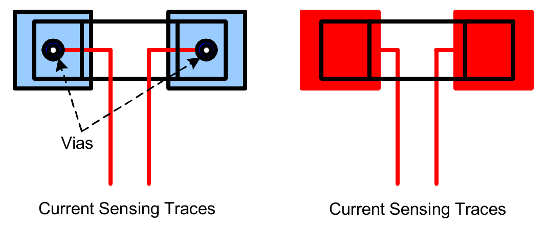 |
| 16 | ADP |
Run this trace with sufficient width in parallel fashion with the ASGATE pin trace. |
| 17 | DCIN |
Place the OR diodes and the RC filter in the general proximity of the controller. Run the VADP trace and VSYS trace to the OR diodes with sufficient width. |
| 18 | VDD |
Place the RC filter connecting with the VDDP pin in the general proximity of the controller. Run the trace connecting to the VDDP pin with sufficient width. |
| 19 | ACIN |
Place the voltage divider resistors and the optional decoupling capacitor in the general proximity of the controller. |
| 20 | OTGEN/CMIN |
No special consideration. |
| 21 22 |
SDASCL |
Digital pins. No special consideration. Run the SDA and SCL traces in parallel. |
| 23 24 |
PROCHOT#ACOK |
Digital pin, open-drain output. No special consideration. |
| 25 | BATGONE |
Digital pin. Place the 100kΩ resistor series in the BATGONE signal trace and the optional decoupling capacitor in the general proximity of the controller. |
| Pin Number | Pin Name | Layout Guidelines |
|---|---|---|
| 26 | OTGPG/CMOUT |
Digital pin, open-drain output. No special consideration. |
| 27 | PROG |
Signal pin. Place the PROG programming resistor in the general proximity of the controller. |
| 28 | COMP |
Place the compensation components in the general proximity of the controller. Avoid any switching signal from crossing over or getting close. |
| 29 | AMON/BMON |
No special consideration. Place the optional RC filter in the general proximity of the controller. |
| 30 | CONFIG/PSYS |
Dual-purpose pin: Configuration input or current source signal output. No special consideration. |
| 31 | VBAT |
Place the optional R-C filter in the general proximity of the controller. Run a dedicated trace from the battery positive connection point to the IC. |
| 32 | BGATE |
Use sufficient width trace from the IC to the BGATE MOSFET gate. Place the capacitor from BGATE to ground close to the MOSFET. |