
4 KiB
5. General SMBus Architecture
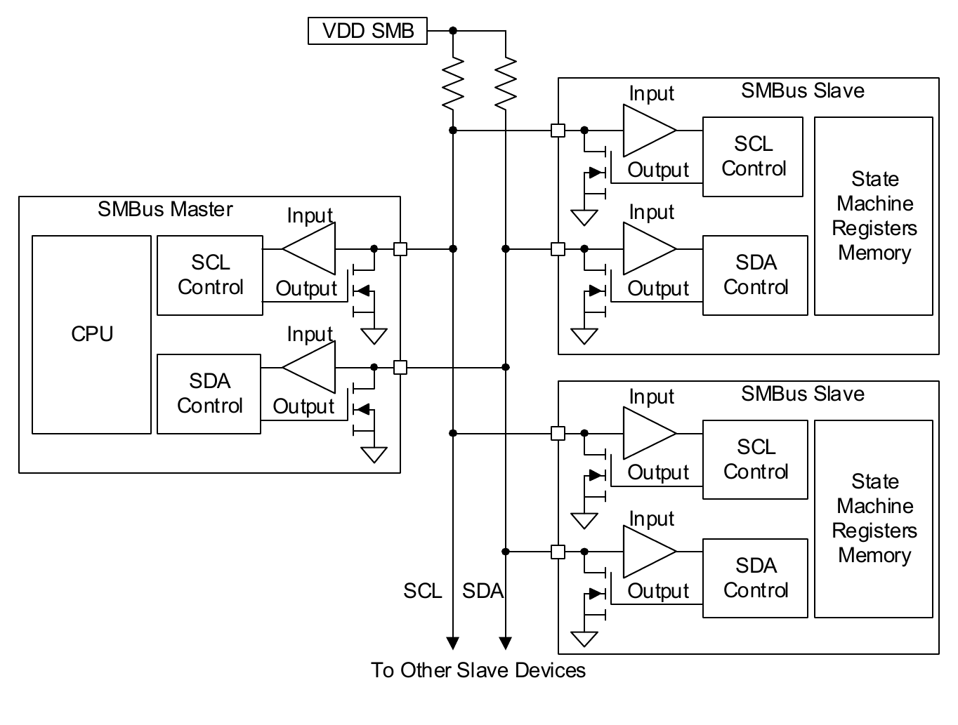
Figure 33. General SMBus
5.1 Data Validity
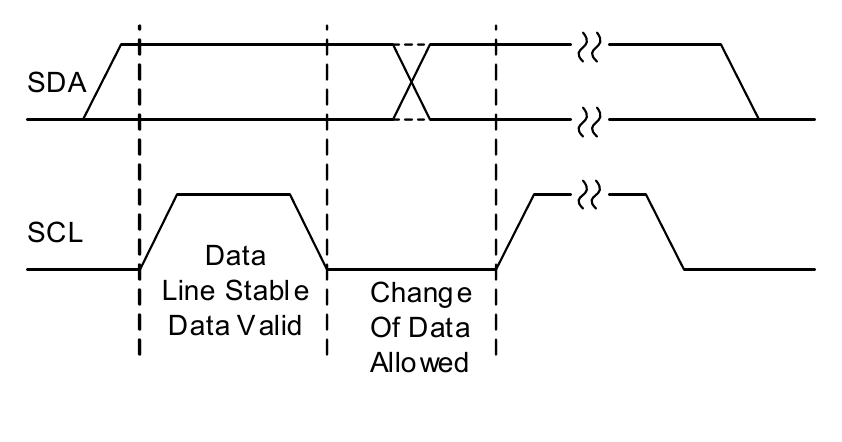
The data on the SDA line must be stable during the HIGH period of the SCL, unless generating a START or STOP condition. The HIGH or LOW state of the data line can change only when the clock signal on the SCL line is LOW. See Figure 34.
Figure 34. Data Validity
5.2 START and STOP Conditions
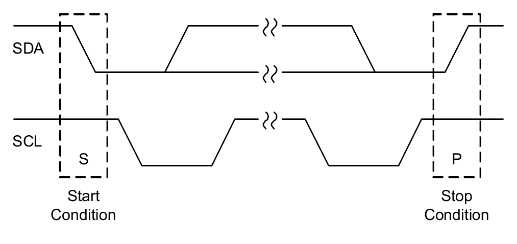
In Figure 35, the START condition is a HIGH to LOW transition of the SDA line while SCL is HIGH.
The STOP condition is a LOW to HIGH transition on the SDA line while SCL is HIGH. A STOP condition must be sent before each START condition.
Figure 35. Start and Stop Waveforms
5.3 Acknowledge
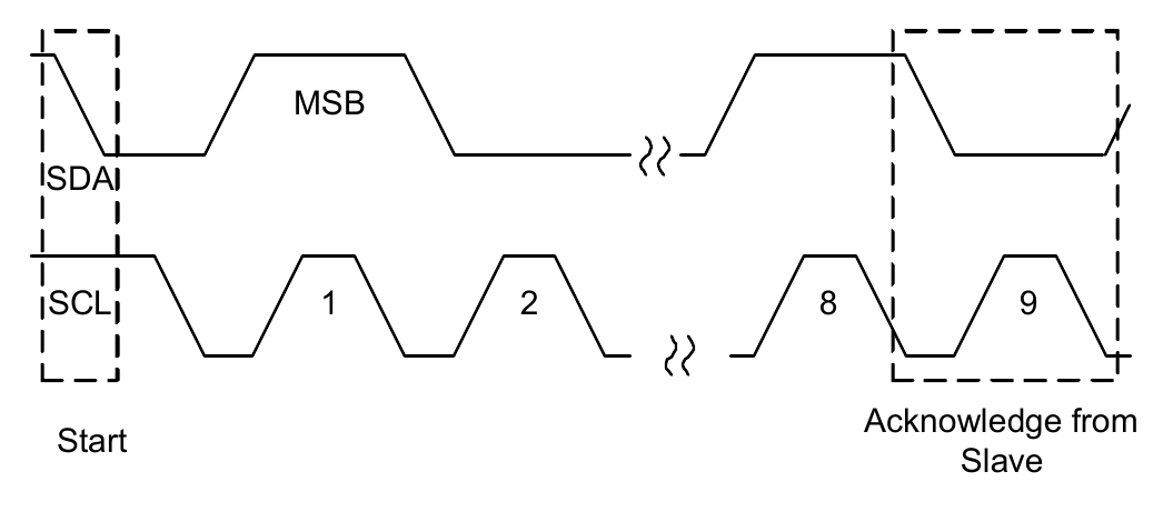
Each address and data transmission uses nine clock pulses. The ninth pulse is the Acknowledge bit (ACK). After the start condition, the master sends seven slave address bits and a R/W bit during the next eight clock pulses. During the ninth clock pulse, the device that recognizes its own address holds the data line LOW to acknowledge (see Figure 36). Both the master and the slave use the ACK bit to acknowledge receipt of register addresses and data.
Figure 36. Acknowledge On The SMBus
5.4 SMBus Transactions
All transactions start with a control byte sent from the SMBus master device. The control byte begins with a Start condition followed by seven bits of slave address (0001001) and the R/W bit. The R/W bit is 0 for a WRITE or 1 for a READ. If any slave device on the SMBus bus recognizes its address, it acknowledges by pulling the Serial Data (SDA) line LOW for the last clock cycle in the control byte. If no slave exists at that address or it is not ready to communicate, the data line is 1 indicating a not acknowledge condition.
When the control byte is sent and the RAA489118 acknowledges it, the second byte sent by the master must be a register address byte such as 0x14 for the ChargeCurrent register. The register address byte tells the RAA489118 which register the master writes or reads. See Table 1 for register details. When the RAA489118 receives a register address byte, it responds with an acknowledge.
5.5 Byte Format
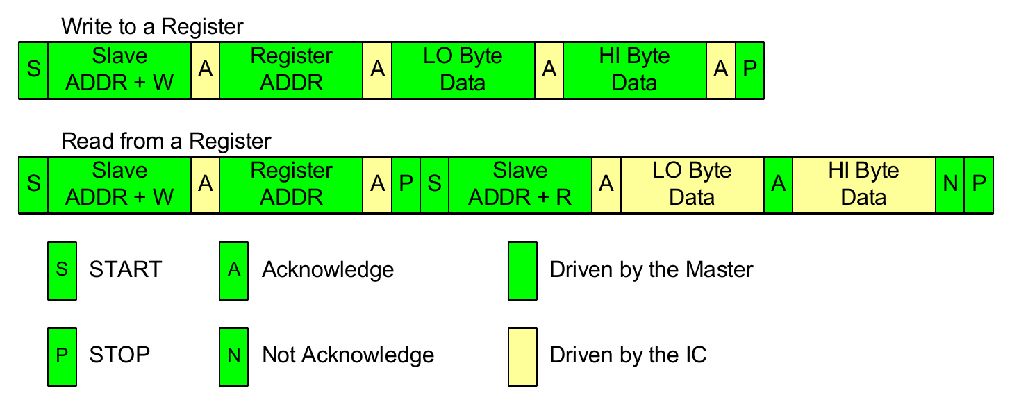
Every byte on the SDA line must be eight bits long and must be followed by an ACK bit. Data is transferred with the Most Significant Bit (MSB) first and the Least Significant Bit (LSB) last. The LO Byte data is transferred before the HI Byte data. For example, when writing 0x41A0, 0xA0 is written first and 0x41 is written second.
Figure 37. SMBus Read and Write Protocol
5.6 SMBus and I2C Compatibility
The RAA489118 SMBus minimum input logic high voltage is 1.3V, so it is compatible with I2C with pull-up power supplies higher than 1.3V.
The RAA489118 SMBus registers are 16 bits, so it is compatible with 16-bit I2C or 8-bit I2C with auto-increment capability.
5.7 SMBus Commands
The RAA489118 receives control inputs from the SMBus interface after Power-On Reset (POR). The serial interface complies with the System Management Bus Specification. The RAA489118 uses the SMBus Read-word and Write-word protocols (see Figure 37) to communicate with the host system and a smart battery. The RAA489118 is an SMBus slave device and does not initiate communication on the bus. It responds to the 7-bit address 0b0001001_ as follows:
The Read and Write address for the RAA489118 is:
- Read address =
0b00010011(0X13H) - Write address =
0b00010010(0X12H)
The data (SDA) and clock (SCL) pins have Schmitt-trigger inputs that can accommodate slow edges. Choose pull-up resistors for SDA and SCL to achieve rise times according to the SMBus specifications.