
28 KiB
5. Functional Description
5.1 Start-Up
When VSYS33 is supplied, 3.3V is supplied to a 3.3V domain block, VSNK_GATE/VSNK_SRC gate driver, and 2.5V LDO. Also, VSYS33 is passed through VDD33. In this condition, the 3.3V LDO is disabled.
When VSYS33 is not supplied and VBUS is supplied, VBUS is the input to the 3.3V LDO and the VSYS33 switch (VSYS33 SW) is turned off. Also, the 3.3V LDO outputs 3.3V to the 3.3V domain block, VSNK_GATE/VSNK_SRC gate driver, 2.5V LDO, and VDD33. This condition is implemented for when the system does not have any power (for example, dead battery condition).
When the output of the 2.5V LDO rises above a 2.4V POR threshold (VDD2p5_2P4_r), the RAA489400 digital block is activated and starts the TCPC operation.
When VDD33 is supplied but both VSYS33 and VBUS are not supplied, 2.5V LDO is not enabled and the RAA489400 does not start the TCPC operation.
When VCONN_POWER is supplied, 5V is supplied to VCONN Mux, charge pump for VCONN, and charge pump for VSRC_GATE/VSRC_SRC/VSRC_BOOT.
5.2 Programming Resistors
A 1% resistor from the PROG pin to GND programs the configuration of the RAA489400.
Table 1 shows the programming option for the SMBus/I²C slave target address. When VDD33 is powered from either VSYS33 or VBUS, RAA489400 checks the resistance value that is connected to PROG pin with GND, and it configures the SMBus/I²C slave target address based on Table 1.
If the RAA489400 receives I²C access before completing a read to the PROG resistor, the RAA489400 ignores the I²C access.
Table 1. PROG Pin Programming Table
| PROG-GND Resistance (Ω) — Min | PROG-GND Resistance (Ω) — Nominal | PROG-GND Resistance (Ω) — Max | Slave Target Address (7-bit) |
|---|---|---|---|
| 950 | 1000 | 1050 | 0x22 |
| 1425 | 1500 | 1575 | 0x23 |
| 2090 | 2200 | 2310 | 0x24 |
| 3135 | 3300 | 3465 | 0x25 |
| 4465 | 4700 | 4935 | 0x26 |
| 6460 | 6800 | 7140 | 0x27 |
5.3 USB Type-C Port Controller Interface
The RAA489400 supports USB Type-C Port Controller Interface specification Revision 2.0 with EPR, which is defined in USB PD specification Revision 3.1. TCPM controls RAA489400 USB Type-C Port Controller through the SMBus/I²C slave target register. Reference the Registers section for details on the TCPC standard and the RAA489400 vendor-defined register information.
5.3.1 USB PD BMC PHY
The RAA489400 supports USB PD BMC (Bi-phase Mark coded) Baseband PHY. The TCPM enables the USB PD BMC PHY when the RAA489400 is in Attached.SNK, Attach.SRC, DebugAccessory with either Source only, Sink only, or the DRP (Dual Role Power) power role, which is configured in ROLE_CONTROL (1Ah). The
RECEIVE_BUFFER (30h) and TRANSMIT_BUFFER (50h) registers are supported to transmit/receive USB PD protocol messages.
5.3.2 USB Type-C Current Mode
The RAA489400 supports the following USB Type-C current options: Default, 1.5A, or 3.0A. This configuration is set in ROLE_CONTROL (1Ah).
5.3.3 VCONN Mux
The VCONN source mux provides 5V power from the VCONN_POWER pin to CC1 or CC2 when Bit0.Enable VCONN in POWER_CONTROL (1Ch) is set to 1b. Bit0.Plug Orientation in TCPC_CONTROL (19h) must be configured for plug orientation when the USB-C device is connected.
When the VCONN fault protection (OV/UV/OT/RV) is enabled and a fault condition is detected, the RAA489400 turns off VCONN Mux.
5V is supplied to VCONN_POWER when the RAA489400 works as a VBUS source.
5.3.4 Source Path Control
RAA489400 supports two options for VBUS source path control. The following options are configured in GPIO1_CTRL Register (82h), GPIO2_CTRL Register (83h), GPIO3_CTRL Register (84h), GPIO4_CTRL Register (85h), VBUS_PATH_CTRL Register (86h), and VBUS_GPIO_CTRL Register (87h).
VSRC_GATE/VSRC_SRC/VSRC_BOOTfor external N-ch MOSFET- GPIO (VBUS source power switch enable function for external VBUS power switch)
When TCPM sends a command of DisableSourceVbus or SourceVbusDefaultVoltage to the RAA489400 through COMMAND (23h), the RAA489400 turns off/on the VBUS source path.
When the VBUS source fault protection (OC/OV/UV/RV) is enabled and a fault condition is detected, RAA489400 turns the VBUS source path off.
5.3.5 Sink Path Control
The RAA489400 supports two options for the VBUS sink path control. The following options are configured in GPIO1_CTRL Register (82h), GPIO2_CTRL Register (83h), GPIO3_CTRL Register (84h), GPIO4_CTRL Register (85h), VBUS_PATH_CTRL Register (86h), and VBUS_GPIO_CTRL Register (87h).
VSNK_GATE/VSNK_SRCfor external N-ch MOSFET- GPIO (VBUS sink power switch enable function for external VBUS power switch)
When the TCPM sends a command of DisableSinkVbus or SinkVbus to the RAA489400 through COMMAND (23h), the RAA489400 turns off/on the VBUS sink path.
When the VBUS sink fault protection (OV/UV) is enabled and a fault condition is detected, the RAA489400 turns off VBUS sink path.
5.3.6 Bi-directional VBUS Source and Sink Path Control
The RAA489400 supports one option for a bi-directional VBUS source and sink path control (see Figure 9). The GPIO must be used to control the bi-directional VBUS source and sink path. VBUS_SRC_SEL and VBUS_SNK_SEL must be set with same value with one GPIO pin in VBUS_PATH_CTRL Register.
For example, VBUS_PATH_CTRL Register is set to 0x33 with GPIO1. In this case, when the TCPM sends a command of SourceVbusDefaultVoltage or SinkVbus to RAA489400, GPIO1 is asserted to turn bi-directional VBUS source and sink path on. When the TCPM sends a command of DisableSourceVbus and DisableSinkVbus to the RAA489400, GPIO1 is deasserted to turn bi-directional VBUS source and sink path off. Because of VBUS protection functions, the TCPM must send an appropriate command to control that is based on CC_STATUS Register.
Note: SRC_VBUS_RVP_DIS must be set to 1b to disable the VBUS reverse voltage protection function when VBUS_SRC_SEL and VBUS_SNK_SEL are set to same value for bi-directional VBUS path control.
5.3.7 VBUS Monitoring and Measurement
The RAA489400 supports the VBUS Monitoring and Measurement function for VBUS voltage, VBUS current, Sink Disconnect Detection, and VBUS Discharge to vSafe0V as described in the following sections.
5.3.7.1 VBUS Voltage Measurement
The TCPM can monitor the VBUS voltage measurement status in VBUS_VOLTAGE (70h) when Bit6.VBUS_VOLTAGE Monitor in POWER_CONTROL (1Ch) is enabled.
5.3.7.2 VBUS Current Measurement
The TCPM can monitor VBUS current measurement status in VBUS_CURRENT Register (92h) when the Disabled VBUS_CURRENT monitor is set to 0b in VBUS_CTRL Register (90h).
The TCPM can also monitor a peak current and average current in VBUS_PEAK_CURRENT Register (94h) and VBUS_AVE_CURRENT Register (96h) when Bit4.PEAK_EN and/or Bit7.AVERAGE_EN is enabled in VBUS_CTRL Register (90h).
VBUS_PEAK_CURRENT Register (94h) shows a maximum VBUS peak current.
VBUS_AVE_CURRENT Register (96h) shows an average current over a time period specified in VBUS_CTRL Register (90h). The RAA489400 calculates the average current as the following. Refer to VBUS_CTRL Register (90h) for more information.
y_n = \text{Average Current at Time } n,\quad x_n = \text{VBUS Current sampled at Time } n,\quad y_0 = 0y_{n+1} = y_n + \frac{(x_n - y_n)}{(N3 \times 2^{N4})}5.3.7.3 VBUS Voltage Alarm
The VBUS voltage alarm function is disabled as a default setting per TCPCi specification. The TCPM can write DisableVoltageAlarms = 0b in POWER_CONTROL (1Ch) to enable the voltage alarms.
The TCPM can write to VBUS_VOLTAGE_ALARM_HI_CFG (76h) to set the high voltage alarm level. The RAA489400 sets VBUSVoltageAlarmHi to 1b in ALERT (10h) when VBUS exceeds the high voltage alarm level in VBUS_VOLTAGE_ALARM_HI_CFG (76h). The RAA489400 re-asserts VBUSVoltageAlarmHi in ALERT (10h) when the high voltage condition on VBUS prevails after the TCPM has cleared VBUSVoltageAlarmHi in ALERT (10h) unless the TCPM disables the voltage alarms by setting DisableVoltageAlarms to 1b in POWER_CONTROL (1Ch).
The TCPM can write to VBUS_VOLTAGE_ALARM_LO_CFG (78h) to set the low voltage alarm level. The RAA489400 sets VBUSVoltageAlarmLo to 1 in ALERT (10h) when VBUS drops below the low voltage alarm level in VBUS_VOLTAGE_ALARM_LO_CFG (78h). The RAA489400 re-asserts VBUSVoltageAlarmLo in ALERT (10h) when the low voltage condition on VBUS prevails after the TCPM has cleared VBUSVoltageAlarmLo in ALERT (10h), unless the TCPM disables the voltage alarms by setting DisableVoltageAlarms to 1b in POWER_CONTROL (1Ch).
5.3.7.4 VBUS Discharge
The RAA489400 supports the automatic VBUS discharge function after a disconnect detection when Bit4.Auto Discharge Disconnect is set to 1b in POWER_CONTROL (1Ch) 1b. The RAA489400 supports force VBUS discharge by setting Bit.2.Force Discharge in POWER_CONTROL (1Ch) so that the TCPM can manually discharge VBUS.
When the RAA489400 starts the VBUS discharge to vSafe0V, the RAA489400 monitors the VBUS voltage and stops the VBUS discharge when VBUS is below vSafe0V (max). When the VBUS discharge is stopped, the RAA489400 does not reapply the VBUS discharge although the VBUS might be higher than vSafe0V (max), but it does reapply the VBUS discharge when another VBUS discharge command or event occurs.
In contrast, when the RAA489400 is the source and the Force Discharge bit of the POWER_CONTROL register is set to 1b, the RAA489400 starts the VBUS discharge and monitors the VBUS voltage to stop the discharging. The discharging VBUS voltage is stopped when the VBUS voltage is below the VBUS_STOP_DISCHARGE_THRESHOLD register.
5.3.8 Internal Sink Path Discharge
The RAA489400 provides an internal Sink discharge function with the SNK_DISCHG pin to discharge an internal sink path, for example, between VBUS sink gate and the battery charger (adapter side).
When a system supports multiple USB-C ports with multiple RAA489400 devices and the first USB-C port (C1) has an EPR Source adapter (up to 240W/48V) and a second USB-C port (C2) has a SPR (up to 100W/20V) source adapter (as in Figure 13), the internal system sink path between the VBUS sink gate and a battery charger (adapter side) has a high voltage (such as 48V). In this case when the EPR source adapter is disconnected, the internal system sink path must be discharged to vSafe5V or 0V for safety before the VBUS sink gate of the second USB-C port is turned on. Otherwise, the SPR source adapter on the second USB-C port might have damage because of a higher voltage than its source capability from the internal sink path.
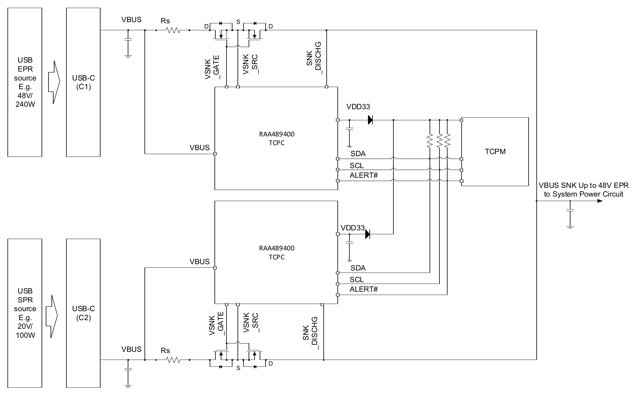
The RAA489400 provides the following option for the TCPM or system when the RAA489400 works as a sink. The following options can be configured in SINK_PATH_DISCHG Register (9Ah).
- Automatic discharge when RAA489400 receives SinkVbus command.
- Manual discharge with TCPM operation.
5.3.8.1 Automatic Discharge
When DISCHG_MODE of SINK_PATH_DISCHG Register (9Ah) is set to 1b (that is automatic discharge), the RAA489400 receives the SinkVbus command and the internal sink path voltage exceeds the vSafe5V(max); the RAA489400 automatically discharges the internal sink path voltage until the voltage reaches below the
vSafe5V(max). When a voltage is lower than the vSafe5V(max), the RAA489400 stops to discharge and enables VBUS sink gate.
The sink discharge timeout is set to DISCHARGE_TIMEOUT of SINK_PATH_DISCHG Register (9Ah) if the internal sink path voltage is higher than the vSafe5V(max) after the sink discharge timeout setting of receiving the SinkVbus command. Next, the RAA489400 sets a 1b sink path discharge completion bit (Bit 14) and a Sink path discharge timeout bit (Bit15) of VENDOR_STATUS Register (A0h) to notify a discharge failure, and it asserts an ALERT# pin to the TCPM. Afterwards, the RAA489400 discards the SinkVbus command. Also, the TCPM can acknowledge the internal sink path has failed to reach the vSafe5V and can report this failure to the EC and/or CPU.
Note: The RAA489400 does not discharge the internal sink path when it detects a disconnection.
5.3.8.2 Manual Discharge
When DISCHG_MODE of SINK_PATH_DISCHG Register (9Ah) is set to 0b (that is manual discharge) and the TCPM writes 1b to MANUAL_DISCHG of SINK_PATH_DISCHG Register (9Ah), the RAA489400 discharges the internal sink path voltage to vSafe5V(max). When a voltage is lower than the vSafe5V(max), the RAA489400 stops discharge and sets 1b to the sink path discharge completion bit (Bit14) of VENDOR_STATUS Register (A0h) to notify discharge completion and assert ALERT# pin to the TCPM. Next, the TCPM can send the SinkVbus command to the RAA489400 that controls the second USB-C port.
The Sink Discharge Timeout of discharge is set to DISCHARGE_TIMEOUT of SINK_PATH_DISCHG Register (9Ah) if the internal sink path voltage is higher than the vSafe5V(max) after the sink discharge timeout setting of receiving the MANUAL_DISCHG = 1b, and the RAA489400 sets 1b to the sink path discharge completion bit (Bit14) and sink path discharge timeout bit (Bit15) of VENDOR_STATUS Register (A0h) to notify discharge failure and assert the ALERT# pin to TCPM. Finally, the TCPM can acknowledge the internal sink path has failed to reach the threshold setting and can report this failure to the EC and/or CPU.
5.3.9 Initial Sink Fast Role Swap
The RAA489400 supports Initial Sink Fast Role Swap based on the USB PD specification. Fast Role Swap can be enabled in POWER_CONTROL (1Ch).
The RAA489400 turns Sink gate off at first when Fast Role Swap occurs, that is when the RAA489400 receives the Fast Role Swap Signal from a connected USB-C/PD VBUS source device. Next, the RAA489400 turns Source gate on for a new sink device.
Trigger conditions of Sink/Source gate control and timing between those controls are defined in FRS_CTRL Register (98h). Settings of this register are valid only when the Fast Role Swap Enable bit of the POWER_CONTROL (1Ch) is set to 1b.
The TCPM must disable the Fast Role Swap in POWER_CONTROL (1Ch) before the TCPM sends a FR_Swap message.
Note: The RAA489400 does not support Initial Source Fast Role Swap.
Note: The RAA489400 does not consider Fast Role Swap support with Bi-directional VBUS Source and Sink Path Control.
5.4 Protection Features
The RAA489400 supports features for VBUS protection and VCONN Mux protection as described in the following sections. Table 2 and Table 3 clarify the control/status/mask register for each protection.
Table 2. VBUS Protection
| Protection | Supported Power Role | Control Register | Status Register | Mask Register |
|---|---|---|---|---|
| VBUS Overcurrent | Source/Sink | FAULT_CONTROL (1Bh) |
FAULT_STATUS (1Fh) |
FAULT_STATUS_MASK (15h) |
| VBUS Overvoltage | Source/Sink | FAULT_CONTROL (1Bh)VBUS_FAULT_CTRL Register (A4h) |
FAULT_STATUS (1Fh) |
FAULT_STATUS_MASK (15h) |
| VBUS Undervoltage | Source | VBUS_FAULT_CTRL Register (A4h) |
VENDOR_STATUS Register (A0h) |
VENDOR_STATUS_ALERT_MASK Register (A2h) |
| VBUS Reverse Voltage | Source | VBUS_FAULT_CTRL Register (A4h) |
VENDOR_STATUS Register (A0h) |
VENDOR_STATUS_ALERT_MASK Register (A2h) |
Table 3. VCONN Protection
| Protection | Control Register | Status Register | Mask Register |
|---|---|---|---|
| VCONN Overcurrent | FAULT_CONTROL (1Bh)VCONN_FAULT_CTRL Register (A6h) |
FAULT_STATUS (1Fh) |
FAULT_STATUS_MASK (15h) |
| VCONN Overvoltage | VCONN_FAULT_CTRL Register (A6h) |
VENDOR_STATUS Register (A0h) |
VENDOR_STATUS_ALERT_MASK Register (A2h) |
| VCONN Undervoltage | VCONN_FAULT_CTRL Register (A6h) |
VENDOR_STATUS Register (A0h) |
VENDOR_STATUS_ALERT_MASK Register (A2h) |
| VCONN Reverse Voltage | VCONN_FAULT_CTRL Register (A6h) |
VENDOR_STATUS Register (A0h) |
VENDOR_STATUS_ALERT_MASK Register (A2h) |
| VCONN Over-temperature | VCONN_FAULT_CTRL Register (A6h) |
VENDOR_STATUS Register (A0h) |
VENDOR_STATUS_ALERT_MASK Register (A2h) |
5.4.1 VBUS Overcurrent Protection
If the VBUS Overcurrent Protection Fault is enabled in FAULT_CONTROL (1Bh), the RAA489400 takes the following actions when the VBUS overcurrent is detected either internally with CSIP/CSIN or externally with the overcurrent input from the GPIO function.
- Turns off the VBUS source gate and discharge VBUS to vSafe0V when the RAA489400 works as a VBUS source.
- Turns off the VBUS sink gate when the RAA489400 works as a VBUS sink.
- Sets the VBUS Overcurrent Protection Fault bit in
FAULT_STATUS (1Fh). - Asserts the
OCP#pin ifVBUS_OCPofOCP_OUTPUT_CTRL Register (A8h)is set to 1b. - If the RAA489400 works as a VCONN source (that is Enable VCONN = 1b in
POWER_CONTROL (1Ch)), the RAA489400 also takes the following actions:- Turns off VCONN Mux and discharges VCONN to vVconnDischarge.
- Clears Enable VCONN to 0b in
POWER_CONTROL (1Ch).
The VBUS overcurrent threshold can be configured in VBUS_FAULT_CTRL Register (A4h). The following threshold setting is available: 3.6A (Default), 1.8A, 4.8V, and 6.0A.
5.4.2 VBUS Overvoltage Protection
If the VBUS Overvoltage Protection Fault is enabled in FAULT_CONTROL (1Bh) and/or VBUS_FAULT_CTRL Register (A4h), the RAA489400 takes the following actions when VBUS overvoltage is detected.
- Turns off the VBUS source gate and discharges VBUS to vSafe0V when the RAA489400 works as a VBUS source
- Turn off the VBUS sink gate when the RAA489400 works as a VBUS sink.
- Sets the VBUS Overvoltage Protection Fault bit in
FAULT_STATUS (1Fh). - Asserts the
OCP#pin if theVBUS_OVPofOCP_OUTPUT_CTRL Register (A8h)is set to 1b. - If RAA489400 works as VCONN source (that is Enable VCONN = 1b in
POWER_CONTROL (1Ch)), the RAA489400 also takes the following actions:- Turns off VCONN Mux and discharges VCONN to vVconnDischarge.
- Clears Enable VCONN to 0b in
POWER_CONTROL (1Ch).
Note: The VBUS source overvoltage thresholds are vVbusOv, vSprMax, or vEprMax in the Electrical Specifications. The VBUS sink overvoltage thresholds are vSprMax or vEprMax in the Electrical Specifications. The VBUS overvoltage threshold is configured in VBUS_FAULT_CTRL Register (A4h).
5.4.3 VBUS Source Undervoltage Protection
If VBUS Source Undervoltage Protection is enabled in the VBUS_FAULT_CTRL Register (A4h), the RAA489400 takes the following when VBUS source undervoltage is detected and RAA489400 works as a VBUS Source.
- Turns off the VBUS source gate and discharges VBUS to vSafe0V.
- Sets
SRC_VBUS_UVPbit inVENDOR_STATUS Register (A0h). - Asserts the
OCP#pin ifSRC_VBUS_UVPofOCP_OUTPUT_CTRL Register (A8h)is set to 1b. - Sets the VBUS Overcurrent Protection Fault bit in
FAULT_STATUS (1Fh)if the VBUS Overcurrent Protection Fault bit inFAULT_CONTROL (1Bh)is set to 0b andVBUS_UVPofOCP_OUTPUT_CTRL Register (A8h)is set to 1b. - If the RAA489400 works as a VCONN source (that is Enable VCONN = 1b in
POWER_CONTROL (1Ch)), the RAA489400 also takes the following actions:- Turns off VCONN Mux and discharges VCONN to vVconnDischarge.
- Clears Enable VCONN to 0b in
POWER_CONTROL (1Ch).
Note: The VBUS source undervoltage detection is not activated from the moment VBUS is enabled to the time specified by UVP_INACTIVE_TIME is elapsed, although the SRC_VBUS_UVP_DIS bit of VBUS_FAULT_CTRL Register (A4h) is 0b and the VBUS voltage is below the vVbusUv threshold.
Note: The RAA489400 does not support the VBUS sink undervoltage when the RAA489400 works as a VBUS sink, because the RAA489400 supports VBUS_SINK_DISCONNECT_THRESHOLD (72h) to detect a disconnection.
5.4.4 VBUS Source Reverse Voltage Protection
If VBUS Source Reverse Voltage Protection is enabled in VBUS_FAULT_CTRL Register (A4h), the RAA489400 takes the following when VBUS RV is detected.
- Turns off VBUS source gate and then discharges VBUS to vSafe0V when the RAA489400 works as a VBUS source.
- Sets the
SRC_VBUS_RVPbit inVENDOR_STATUS Register (A0h). - Asserts the
OCP#pin ifVBUS_RVPofOCP_OUTPUT_CTRL Register (A8h)is set to 1b. - Sets the VBUS Overcurrent Protection Fault bit in
FAULT_STATUS (1Fh), if the VBUS Overcurrent Protection is enabled inFAULT_CONTROL (1Bh)andVBUS_RVPofOCP_OUTPUT_CTRL Register (A8h)is set to 1b.
- If the RAA489400 works as a VCONN source (that is Enable VCONN = 1b in
POWER_CONTROL (1Ch)), the RAA489400 also takes the following actions:- Turns off VCONN Mux and discharges VCONN to vVconnDischarge.
- Clears Enable VCONN to 0b in
POWER_CONTROL (1Ch).
Note: When VBUS_SRC_SEL and VBUS_SNK_SEL are set to the same value in VBUS_PATH_CTRL Register for bi-directional VBUS path control, the VBUS source reverse voltage protection must be disabled.
5.4.5 VCONN Overcurrent Protection
If the VCONN Overcurrent Fault is enabled in FAULT_CONTROL (1Bh), the RAA489400 takes the following when the VCONN Overcurrent is detected.
- Clears Enable VCONN to 0b in
POWER_CONTROL (1Ch). - Turns off VCONN Mux and discharges VCONN to vVconnDischarge.
- Sets the VCONN Overcurrent Fault bit in
FAULT_STATUS (1Fh). - Asserts the
OCP#pin ifVCONN_OCPofOCP_OUTPUT_CTRL Register (A8h)is set to 1b.
The VCONN overcurrent threshold is configured in the VCONN_FAULT_CTRL Register (A6h). The following threshold setting is available: 400mA (default), 600mA, and 800mA.
5.4.6 VCONN Overvoltage Protection
The RAA489400 takes the following when VCONN overvoltage is detected.
- Clears Enable VCONN to 0b in
POWER_CONTROL (1Ch). - Turns off VCONN Mux and discharges VCONN to vVconnDischarge.
- Sets the
VCONN_OVPbit inVENDOR_STATUS Register (A0h). - Asserts the
OCP#pin ifVCONN_OVPofOCP_OUTPUT_CTRL Register (A8h)is set to 1b. - Sets the VCONN Overcurrent Fault in
FAULT_STATUSRegister, if the VCONN Overcurrent Fault is enabled inFAULT_CONTROL (1Bh)andVCONN_OVPofOCP_OUTPUT_CTRL Register (A8h)is set to 1b.
5.4.7 VCONN Undervoltage Protection
The RAA489400 takes the following when VCONN UV is detected.
- Clears Enable VCONN to 0b in
POWER_CONTROL (1Ch). - Turns off the VCONN Mux and discharges VCONN to vVconnDischarge.
- Sets the
VCONN_UVPbit inVENDOR_STATUS Register (A0h). - Asserts the
OCP#pin ifVCONN_UVPofOCP_OUTPUT_CTRL Register (A8h)is set to 1b. - Sets the VCONN Overcurrent Fault bit in
FAULT_STATUS (1Fh), if the VCONN Overcurrent Fault is enabled inFAULT_CONTROL (1Bh)andVCONN_UVPofOCP_OUTPUT_CTRL Register (A8h)is set to 1b.
Note: VCONN_UV detection is not activated from the moment VCONN is enabled to the time specified by UVP_INACTIVE_TIME of VCONN_FAULT_CTRL Register (A6h) is elapsed, although, VCONN_UVP_DIS bit of VCONN_FAULT_CTRL Register (A6h) is 0b and VCONN voltage is below the vVconnUv threshold.
5.4.8 VCONN Over-temperature Protection
If the VCONN Overtemperature Fault is enabled in VCONN_FAULT_CTRL Register (A6h), the RAA489400 takes the following when VCONN OT is detected.
- Clears Enable VCONN to 0b in
POWER_CONTROL (1Ch). - Turns off VCONN Mux and discharges VCONN to vVconnDischarge.
- Turns off the VBUS source gate and discharges VBUS to vSafe0V when the RAA489400 works as a VBUS source.
- Turns off the VBUS sink gate when the RAA489400 works as a VBUS sink.
- Sets the
VCONN_OTPbit inVENDOR_STATUS Register (A0h). - Asserts the
OCP#pin ifVCONN_OTPofOCP_OUTPUT_CTRL Register (A8h)is set to 1b.
5.4.9 VCONN Reverse Voltage Protection
RAA489400 takes the following when VCONN RV is detected.
- Clears Enable VCONN to 0b in
POWER_CONTROL (1Ch) - Turns off VCONN Mux and then discharge VCONN to vVconnDischarge.
- Turns off VBUS source gate and then discharge VBUS to vSafe0V when RAA489400 works as VBUS source.
- Turns off VBUS sink gate when RAA489400 works as VBUS sink.
- Sets
VCONN_RVPbit inVENDOR_STATUS Register (A0h). - Asserts
OCP#pin ifVCONN_RVPof is set to 1b. - Sets the VCONN Overcurrent Fault bit in
FAULT_STATUS (1Fh), if the VCONN Overcurrent Fault is enabled inFAULT_CONTROL (1Bh)andVCONN_RVPofOCP_OUTPUT_CTRL Register (A8h)is set to 1b.
5.5 OCP# Output
When RAA489400 detects a fault condition which is configured in OCP_OUTPUT_CTRL Register (A8h), the RAA489400 asserts the OCP# pin to low. When all fault conditions are removed in FAULT_STATUS (1Fh) and VENDOR_STATUS Register (A0h), the RAA489400 deasserts OCP# pin.
The OCP# function is used for a direct notification signal from the RAA489400 to a system (such as a power management circuit or main system SoC) to notify a fault event.
5.6 PROCHOT#
RAA489400 supports the PROCHOT# function to notify disconnection of a VBUS source device and/or fast role swap event. If the PROCHOT function is enabled in PROCHOT_EN Register (AAh), the RAA489400 asserts PROCHOT# when the RAA489400 detects the following conditions based on the configuration in PROCHOT_EN Register (AAh).
- Disconnection of VBUS source device.
- FRS signal received.
For example, the PROCHOT# function is used for a direct notification signal from the RAA489400 to a system (such as a power management circuit or main system SoC) in the event that a USB-C port loses a power source so that a system starts to reduce a VBUS current drawing.
Table 4. PROCHOT# Assertion Condition for the Event of Disconnection of VBUS Source Device
PROCHOT_EN SNK_DETACH_EN |
SNK_DETACH SNK_OPEN |
VENDOR_STATUS SNK_DETCH_PROCHOT |
PROCHOT# signal |
|---|---|---|---|
| 0 | Zero | Set to 1b | Deasserted |
| 0 | Non-Zero | Set to 1b | Deasserted |
| 1 | Zero | Set to 1b | Deasserted |
| 1 | Non-Zero | Set to 1b | Asserted |
Table 5. PROCHOT# Assertion Condition for the Event of FRS Signal Received
PROCHOT_EN FRS_EN |
POWER_CONTROL Fast Role Swap Enable |
ALERT_EXTERNED Sink Fast Role Swap |
PROCHOT# signal |
|---|---|---|---|
| 0 | 0b | Set to 0b | Deasserted |
| 0 | 1b | Set to 0b | Deasserted |
| 1 | 0b | Set to 0b | Deasserted |
| 1 | 1b | Set to 1b | Asserted |
5.7 GPIO
The RAA489400 supports the configurable general-purpose input and output with the following functions. The following function can be configured in GPIO1_CTRL Register (82h), GPIO2_CTRL Register (83h), GPIO3_CTRL Register (84h), GPIO4_CTRL Register (85h), VBUS_PATH_CTRL Register (86h), VBUS_GPIO_CTRL Register (87h), and GPIO_OC_EN Register (89h).
- VBUS source power switch enable function (see Source Path Control).
- VBUS sink power switch enable function (see Sink Path Control).
- Overcurrent Input (as
STANDARD_INPUTin TCPCI specification). (See Overcurrent Input.) - General purpose input.
- General purpose output (push-pull).
- General Purpose output (open-drain).
5.7.1 Overcurrent Input
The RAA489400 supports the Overcurrent Input function that is defined in STANDARD_INPUT_CAPABILITIES Register as a TCPCi specification to detect a fault condition from an external VBUS power switch.
An input status is shown in GPIO1_CTRL Register (82h), GPIO2_CTRL Register (83h), GPIO3_CTRL Register (84h), and/or GPIO4_CTRL Register (85h) as well as FAULT_STATUS (1Fh) for the TCPM when a GPIO is enabled as an Overcurrent Input function in GPIO_OC_EN Register (89h).
In addition, if a fault condition is detected from an external VBUS power switch, a GPIO is enabled as an Overcurrent Input function in GPIO_OC_EN Register (89h), and the OCP# output is enabled in OCP_OUTPUT_CTRL Register (A8h), the RAA489400 asserts the OCP# pin to low.
5.8 Clock Management
The RAA489400 supports the integrated oscillators for a 30kHz and 24MHz internal clock. The 30kHz oscillator always works. The 24MHz oscillator can be disabled by the TCPM with the Stop_24MHz_OSC bit in TYPE_C_PRAMETER Register (E2h) when no USB-C device is connected to the RAA489400. When CC1/CC2 status is changed or I²C access is received, the 24MHz clock is automatically enabled and the Stop_24MHz_OSC bit is automatically cleared in TYPE_C_PRAMETER Register (E2h). The Stop_24MHz_OSC bit in TYPE_C_PRAMETER Register (E2h) reduces power consumption.