
28 KiB
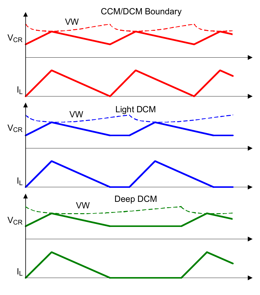
Figure 46. Period Stretching
8. Application Information
8.1 Soft-Start
The RAA489118 includes a low power LDO with nominal 4.6V output, with an input OR-ed from the VBAT and ADP pins. The RAA489118 also includes a high power LDO with nominal 5V output, with an input from the DCIN pin, which connects to both the adapter and the system bus through an external OR-ing diode circuit. Both LDO outputs are tied to the VDD pin to provide the bias power and gate drive power for the RAA489118. The VDDP pin is the RAA489118 gate drive power supply input. Use an R-C filter to generate the VDDP pin voltage from the VDD pin voltage.
When VDD > 2.7V, the digital block is activated and the SMBus register is ready to communicate with the master controller.
With VADP >3.2V and after the 1.3s or 150ms debounce time, the RAA489118 uses a patented Renesas technique to check whether the input bus is shorted. If CSIP <2V or ACIN <0.8V, ASGATE does not turn on. The input bus short protection adds an additional few milliseconds of delay, wherein the delay depends on the input capacitance. For adapter insertions after the initial one, the debounce time of 1.3s or 150ms is set by Control2 register Bit[11]. The debounce time for an initial adapter insertion is always 150ms. After the debounce time and the input bus short check, ASGATE starts turning on with 10µA of sink current.
Use a voltage divider from the adapter voltage to set the ACIN pin voltage. The RAA489118 monitors the ACIN pin voltage to determine the presence of the adapter. When VDD > 3.8V, the ACIN pin voltage exceeds 0.6V, and ASGATE is fully turned on, the RAA489118 allows the external circuit to pull up the ACOK pin. When ACOK is asserted, the RAA489118 starts switching.
The ACOK is an open-drain output pin that indicates the presence and readiness of the adapter to supply power to the system bus. The RAA489118 actively pulls ACOK low in the absence of the adapter.
Before ASGATE turns ON, the RAA489118 sources 10µA of current out of the PROG pin and reads the pin voltage to determine the PROG resistor value. The PROG resistor programs the configurations of the RAA489118.
In Battery Only mode, the RAA489118 enters Low Power mode if only the battery is present. VDD is 4.6V from the low power LDO to minimize power consumption.
8.2 Charging Mode Configuration
The RAA489118 can be configured to support a battery-charging-only application with no requirement for a battery FET (BFET). Connecting the CONFIG/PSYS pin to VDD configures the Buck-Boost charger to operate with no BFET. To configure the RAA489118 to support operation with a BFET, the CONFIG/PSYS pin should be pulled to ground with a PSYS resistor. For this case, the CONFIG/PSYS pin provides PSYS functionality.
CONFIG/PSYStied to VDD: Battery-charging-only mode with no BFETCONFIG/PSYSconnected to PSYS resistor: NVDC charging with BFET support
8.2.1 Battery Charging Only (no BFET)
Figure 2 provides a circuit topology for an application that has no BFET, and which only provides battery charging. With no BFET, the system bus (VSYS) cannot be isolated from the battery (VBAT), and VSYS cannot be regulated separately from VBAT. With CONFIG/PSYS tied to VDD, the Buck-Boost charger is configured to support such a battery-charging-only application that has no BFET.
At POR with CONFIG/PSYS tied to VDD, the Charge Current (CC) DAC register (0x14) is initialized to 256mA (presuming Rs2 = 5 mΩ), and the charging mode is set for SMBus control (Control3 Bit[7] = 1). This causes the Buck-Boost charger to begin operation by charging an attached battery at the relatively low level of 256 mA. In typical usage, the charge current would be increased after initialization by writing a new value to the CC DAC register (0x14).
In battery-charging-only mode, there is no SMBus timeout function. Charging continues indefinitely and does not require any I2C interaction.
Note: Maintain the CC register at a nonzero value, because setting CC to zero disables the charge current limit.
8.2.2 NVDC Charging (with BFET)
Figure 3 provides a circuit topology for an application that has a BFET, which supports NVDC battery charging. The BFET provides the ability to isolate the system bus (VSYS) from the battery (VBAT), such that VSYS can be regulated independently of VBAT. With CONFIG/PSYS connected to a PSYS resistor, the Buck-Boost charger supports NVDC charging with a BFET.
If CONFIG/PSYS is connected to a PSYS resistor, the Charge Current DAC register (0x14) is initialized with 0A at POR. The BFET is turned off so that there is no battery charge current. The Buck-Boost charger initializes to CV control, such that VSYS is regulated at the MaxSystemVoltage level. Battery charging can be subsequently enabled by writing a nonzero value to the CC DAC register (0x14).
8.3 Programming Charger Option
The resistor from the PROG pin to GND programs the default number of battery cells in series, the default AdapterCurrentLimit1 register value, and the autonomous charging function. Table 16 shows the programming options.
Table 16. PROG Pin Programming Options
| PROG-GND Resistance (kΩ) — Min | PROG-GND Resistance (kΩ) — Typ. 1% | PROG-GND Resistance (kΩ) — Max | Min VSYS (V) | Max VSYS (V) | Autonomous Charging[1] | Default ACLimit1 Reg (A) |
|---|---|---|---|---|---|---|
| 42.7 | 43.2 | 43.7 | 5.12 | 8.400 | Yes | 1.504 |
| 51.7 | 52.3 | 52.9 | 5.12 | 8.400 | No | 1.504 |
| 61.2 | 61.9 | 62.6 | 5.12 | 8.400 | No | 0.48 |
| 70.6 | 71.5 | 72.4 | 7.68 | 12.608 | Yes | 1.504 |
| 81.5 | 82.5 | 83.5 | 7.68 | 12.608 | No | 1.504 |
| 92 | 93.1 | 94.2 | 7.68 | 12.608 | No | 0.48 |
| 104 | 105 | 106 | 10.24 | 16.800 | Yes | 1.504 |
| 116 | 118 | 120 | 10.24 | 16.800 | No | 1.504 |
| 131 | 133 | 135 | 10.24 | 16.800 | No | 0.48 |
| 145 | 147 | 149 | 12.80 | 21.008 | Yes | 1.504 |
| 160 | 162 | 164 | 12.80 | 21.008 | No | 1.504 |
| 176 | 178 | 180 | 12.80 | 21.008 | No | 0.48 |
| 194 | 196 | 198 | 15.36 | 25.200 | Yes | 1.504 |
| 212 | 215 | 218 | 15.36 | 25.200 | No | 1.504 |
| 234 | 237 | 240 | 15.36 | 25.200 | No | 0.48 |
| 258 | 261 | 264 | 17.92 | 29.408 | Yes | 1.504 |
| 284 | 287 | 290 | 17.92 | 29.408 | No | 1.504 |
| 312 | 316 | 320 | 17.92 | 29.408 | No | 0.48 |
- Autonomous charging mode is only configured if CONGIG/PSYS pin is pulled low at POR. If CONFIG/PSYS is tied high at POR, the charging mode is set to SMBus Charging regardless of the PROG resistance.
RAA489118 uses the default MaxVsystemVoltage register values in Table 1. The default switching frequency is 732kHz. If PSYS function is used, battery cell numbers can be mapped as 2/3/4/5/6/7cells versus 8.4/12.6/16.8/21/25.2/29.4V accordingly in Table 1.
The switching frequency can be changed through SMBus Control1 register Bit[9:8] after POR. See the SMBus Control1 register programming table (Table 4) for a detailed description.
Before ASGATE turns on, the RAA489118 sources 10µA of current out of the PROG pin and reads the PROG pin voltage to determine the resistor value. However, application environmental noise can pollute the PROG pin voltage and cause incorrect readings. If noise is a concern, connect a capacitor from the PROG pin to GND to provide filtering. The resistor and the capacitor RC time constant should be less than 40µs so the PROG pin voltage can rise to steady state before the RAA489118 reads it.
If the RAA489118 is powered up from the battery, it does not read the PROG resistor unless PSYS is enabled through SMBus Control1 register Bit[3]. Whenever PSYS is enabled in Battery Only mode, the RAA489118 reads the PROG pin resistor and resets the configuration to the default.
When the adapter is plugged in, the RAA489118 resets the AdapterCurrentLimit1 register to the default by reading the PROG pin resistor if it was not read before, or by loading the previous readings. If PSYS is not enabled, the RAA489118 resets the MaxSystemVoltage register and MinSystemVoltage register to their default values according to the PROG pin setting. If PSYS is enabled, the RAA489118 keeps the values in these two registers.
By default, the adapter current sensing resistor Rs1 is 10mΩ and the battery current sensing resistor Rs2 is 5mΩ. Using this R1 = 10mΩ and Rs2 = 5mΩ option results in an 8mA/LSB correlation in the SMBus current commands. If the Rs1 and Rs2 differ from these default options, the SMBus command needs to be scaled accordingly to obtain the correct current. Smaller current sense resistor values reduce power loss while larger current sense resistor values give better accuracy.
8.4 Autonomous Charging Mode
Autonomous charging mode is only available in the NVDC charging configuration (CONFIG/PSYS pin pulled low at POR).
Autonomous Charging mode can be enabled or disabled through the programming charging option resistor or SMBus Control3 register Bit[7]. When Autonomous Charging mode is enabled, this mode can also be disabled by writing to the SMBus ChargeCurrentLimit or MaxSystemVoltage registers.
The RAA489118 enters Autonomous Charging mode when both the battery voltage is lower than MaxSystemVoltage - 180mV per cell for 1ms of debounce time and the BGATE MOSFET is on.
In Autonomous Charging mode, the RAA489118 starts to charge the battery with 4A (with RS2 = 5mΩ), the PROCHOT# pin (Autonomous Charging mode indication pin) is pulled down to GND, and the SMBus charging timeout timer is disabled. The RAA489118 exits from Autonomous Charging mode when the battery charging current is less than 280mA (with RS2 = 5mΩ) for 20ms or 200ms in CV loop. The autonomous charging termination time can be set by Control3 register Bit[13]. The RAA489118 re-enters Autonomous Charging mode when the battery voltage is discharged below MaxSystemVoltage - 180mV per cell. When the RAA489118 stays in Autonomous Charging mode for 12hrs, which means the battery charging current is higher than 280mA and the battery cannot be charged to MaxSystemVoltage for 12hrs, the RAA489118 stops charging the battery and exits Autonomous Charging mode.
8.5 Battery Ship Mode
The RAA489118 supports Battery Ship mode. When Control3 register Bit[10] is 1, the BGATE MOSFET stays off for Battery Ship mode.
Battery Ship mode sets the lowest power state for the IC. Ship mode can only be entered from Battery Only mode. To achieve the lowest power, several analog functions must be disabled. Many are disabled by default and do not need to be written, but all are listed for completeness. However, the power level can be customized for the system.
- Control1
0x3C- Bit[5] = 1 Disable IMON
- Bit[3] = 0 Disable PSYS
- Control2
0x3D- Bit[3] = 1 Disable GP Comparator
- Control3
0x4C- Bit[10] = 1 Force BGATE Off
To exit Battery Ship mode, use the SMBus to change the control bits.
8.6 Diode Emulation Operation
In Diode Emulation (DE) mode, the RAA489118 uses a phase comparator to monitor the PHASE node voltage during the low-side switching FET on-time to detect the inductor current zero crossing. The phase comparator needs a minimum on-time of the low-side switching FET to recognize inductor current zero crossing. If the low-side switching FET on-time is too short for the phase comparator to successfully recognize the inductor zero crossing, the RAA489118 can lose DE ability. To prevent this, the RAA489118 uses a minimum low-side switching FET on-time. When the intended low-side switching FET on-time is shorter than the minimum value, the
RAA489118 stretches the switching period to keep the low-side switching FET on-time at the minimum value, which causes the CCM switching frequency to drop below the set point.
8.7 Battery Learn Mode
Use Battery Learn mode to supply the system power from the battery even when the adapter is plugged in, such as calibration of the battery fuel gauge.
The RAA489118 enters Battery Learn mode when it receives the SMBus Control command. When entering Battery Learn mode, the RAA489118 turns on the BGATE FET.
In Battery Learn mode, the RAA489118 turns on BGATE and keeps ASGATE on but turns off the buck-boost switcher regardless of whether the adapter is present.
The three ways of exiting Battery Learn mode are:
- Receive the Battery Learn mode exit command through SMBus
- The battery voltage is less than MinSystemVoltage register setting and Control1 Bit[13] = 1
- The
BATGONEpin voltage goes from logic LOW to HIGH
In all these cases, the RAA489118 resumes switching immediately to supply power to the system bus from the adapter to prevent system voltage collapse.
Renesas recommends to disable the slew rate control (Control6 Bit[6] = 0) when using Learn mode.
8.8 Charger Timeout
The RAA489118 includes a timer to ensure the SMBus master is active and to prevent overcharging the battery. The charger timeout functionality is only available in the NVDC charging configuration (CONFIG/PSYS pulled low with PSYS resistor). The RAA489118 terminates charging by turning off the BGATE FET if the charger has not received a write command to the MaxSystemVoltage or ChargeCurrent register within 175s (SMBus Control3 register Bit[12:11] = 00). The charger timeout time can be configured through SMBus Control3 register Bit[12:11]. When charging is terminated by the timeout, the ChargeCurrent register retains its value instead of resetting to zero. If a timeout occurs, the MaxSystemVoltage or ChargeCurrent register must be written to re-enable charging.
The charger timeout function can be disabled using SMBus Control0 register Bit[7] as shown Table 3.
8.9 Monitoring
8.9.1 Current Monitor
The RAA489118 provides an adapter current monitor/OTG current monitor or a battery charging current monitor/battery discharging current monitor through the AMON/BMON pin. The AMON output voltage is 18x (CSIP - CSIN) and 18x (CSIN - CSIP) voltage. The BMON output voltage is 18x (CSON - CSOP) and 36x (CSOP - CSON) voltage.
The AMON and BMON functions can be enabled or disabled through SMBus Control1 register Bit[5]. AMON or BMON can be selected through SMBus Control1 register Bit[4] and the AMON/BMON direction can be configured through SMBus Control3 register Bit[3] as Table 4 shows.
8.9.2 PSYS Monitor
The RAA489118 PSYS pin provides a measure of the instantaneous power consumption of the entire platform. The PSYS pin outputs a current source described by Equation 1.
(EQ. 1) I_{PSYS} = K_{PSYS} \times (V_{ADP} \times I_{ADP} + V_{BAT} \times I_{BAT})
KPSYS is based on the current sensing resistor Rs1 = 10mΩ and Rs2 = 5mΩ. VADP is the adapter voltage in V, IADP is the adapter current in A, VBAT is the battery voltage, and IBAT is the battery discharging current. When the
battery is discharging, IBAT is a positive value; when the battery is being charged, IBAT is a negative value. The battery voltage VBAT is detected through the CSON pin to maximize the power monitor accuracy in NVDC configuration Trickle Charge mode.
The Rs1 to Rs2 ratio must be 2:1 for valid power calculation. If the resistance values are higher (or lower) than the suggested values mentioned previously, KPSYS is proportionally higher (or lower). As an example, if Rs1 = 5mΩ and Rs2 = 2.5mΩ, the output current is half that above for the same power. If the PSYS information is not needed, any Rs1:Rs2 ratio is acceptable.
The default PSYS gain is set to 0.236µA/W, and can be configured through SMBus Control3 register Bit[9].
The PSYS information includes the power loss of the charger circuit and the actual power delivered to the system. The resistor RPSYS connected between the PSYS pin and GND converts the PSYS information from current to voltage.
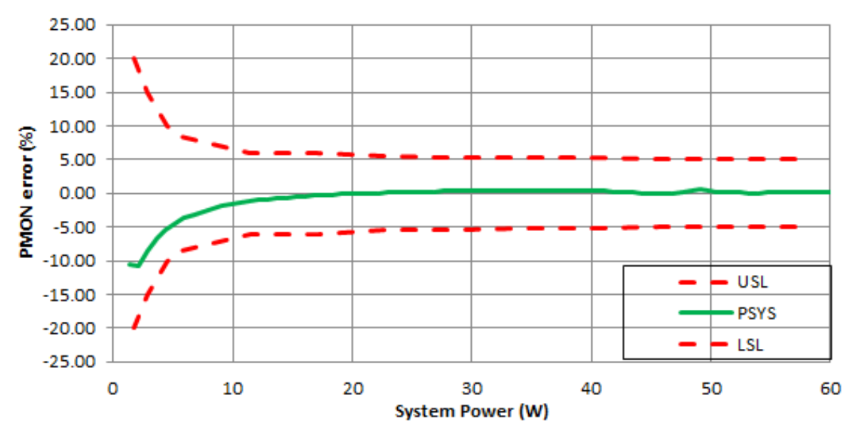
PSYS accuracy limits and a typical accuracy scan are shown in Figure 47.
Figure 47. PSYS Accuracy and Limits
The PSYS function can be enabled or disabled through SMBus Control1 register Bit[3] as shown in Table 4.
8.9.3 PROCHOT#
PROCHOT# is an open-drain output used to support IMVP protocols. A PROCHOT# assertion is triggered if the adapter current exceeds the ACProchot# threshold, the battery discharge current exceeds a discharge current threshold, or VSYS falls below the Low_VSYS_Prochot# threshold. PROCHOT# can also, optionally, be asserted if the OTG Current exceeds a threshold, or by the BATGONE, ACOK, or General Purpose Comparator signals.
In Autonomous Charging mode, the PROCHOT# pin behaves as an indication pin and is pulled down to GND while autonomous-mode charging is active.
8.9.3.1 PROCHOT# for Adapter Overcurrent Conditions
To set the PROCHOT# assertion threshold for adapter overcurrent conditions, write a 16-bit ACProchot# command to register address 0x47 using the Write-word protocol shown in Figure 37 and the data format shown in Table 2. The ACProchot# register can be read back to verify its contents.
If the adapter current exceeds the ACProchot# register setting, the PROCHOT# signal asserts after the debounce time set by Control2 register Bit[10:9]. The PROCHOT# signal remains asserted for a minimum duration set by Control2 register Bit[8:6].
8.9.3.2 PROCHOT# for Battery Over Discharging Current Conditions
The threshold for the PROCHOT# Battery over-discharge condition depends on whether the battery charger is in low-power battery-only mode or in normal mode.
In normal mode, the PROCHOT# signal assertion threshold for battery over discharging current conditions is set by the DCProchot# value in DAC register 0x48.
In battery-only low-power mode with PSYS disabled, the battery over-discharging threshold is set by the DCProchot# level configured by Control0 register Bit[4:3] and Control7 register Bit[1]. However, if PSYS is enabled, the DCProchot# threshold is set by the value in DAC register 0x48.
If the battery discharging current exceeds the DCProchot# threshold, as set by the DCProchot# DAC register 0x48 or Control0 register Bit[4:3] and Control7 register Bit[1], the PROCHOT# signal asserts after the debounce time programmed by Control2 register Bit[10:9]. The PROCHOT# signal remains asserted for a minimum duration time determined by Control2 register Bit[8:6].
8.9.3.3 Low_VSYS_Prochot#
The Low_VSYS_Prochot# threshold is configured using Control1 register Bit[1:0], which provides four threshold settings. In battery-only mode, Low_VSYS_Prochot# only works if PSYS, or OTG is enabled.
8.9.3.4 Other PROCHOT# Triggers
The PROCHOT# signal can also be asserted if the OTG current is excessive, if BATGONE goes high (indicating no battery), if ACOK goes low (indicating no adapter) or if the General-Purpose Comparator triggers. Control4 Bits[7:4] are used to enable these additional PROCHOT# triggers. The OTGCurrent PROCHOT# threshold is the same as the adapter current PROCHOT# threshold ACProchot# specified in DAC register 0x48.
8.9.3.5 Setting PROCHOT# Debounce Time and Duration Time
The PROCHOT# signal debounce time for ACProchot# and DCProchot# is set by Control2 register Bit[10:9]. The low system (VSYS_LOW) voltage PROCHOT# has a fixed debounce time of 7µs.
The minimum duration of a PROCHOT# assertion triggered by Low_VSYS, ACProchot#, or DCProchot# is set by Control2 register Bit[8:6].
The debounce time for PROCHOT# assertions triggered by ACOK and BATGONE is set by Control4 register Bit[3:2].
8.9.3.6 Setting PROCHOT# Clear and Latch Control Bits
Control4 Bit[0] can be used to configure PROCHOT# to latch and hold its state. A latched PROCHOT# assertion can be cleared using Control4 Bit[1].
8.10 Stand-Alone Comparator
The RAA489118 includes a general purpose stand-alone comparator. The OTGEN/CMIN pin is the comparator input. The internal comparator reference is connected to the inverting input of the comparator and can be configured as 1.2V or 2V through SMBus Control2 register Bit[4]. The comparator output is the OTGPG/CMOUT pin. The output polarity can be configured through the SMBus register bit.
- When Control2 register Bit[2] = 0 for normal comparator output polarity, CMOUT = High if CMIN > Reference; CMOUT = Low if CMIN < Reference.
- When Control2 register Bit[2] = 1 for inversed comparator output polarity, CMOUT = Low if CMIN > Reference; CMOUT = High if CMIN < Reference.
By default in Battery Only mode, the stand-alone comparator is enabled. This comparator can be enabled/disabled in Battery Only mode using Control 2 Bit[3]. In Battery Only mode, the reference is always 1.2V, regardless of the value of Control2 Bit[4].
Table 17 shows the OTG mode and the stand-alone comparator truth table.
Table 17. OTG and Comparator Truth Table
| Control1 Bit[11] OTG Function Enable/Disable | Control2 Bit[3] GP Comparator Enable/Disable | PIN-20 OTGEN/CMIN |
PIN-26 OTGPG/CMOUT |
Description |
|---|---|---|---|---|
| 0 | 0 | Comparator Input Pin CMIN | Comparator Output Pin CMOUT | OTG function is disabled. Comparator is enabled. |
| 0 | 1 | X | X | Both the OTG function and comparator are disabled. |
| 1 | 0 | Comparator Input Pin CMIN | Comparator Output Pin CMOUT | Both the OTG function and comparator are enabled. OTG function is enabled when VBAT > 4.5V and Control1 register Bit[11] = 1 without OTG power-good pin indication. The device is in OTG mode while Information1 register 0x3A Bit[6:5] = 11. |
| 1 | 1 | OTG Enable Input Pin OTGEN | OTG Power-Good Indication Pin OTGPG | Comparator is disabled. OTG function is enabled when VBAT > 4.5V and ENOTG pin = High and Control1 register Bit[11] = 1. |
8.11 Protections[1]
8.11.1 Adapter Overvoltage Protection
If the ADP pin voltage exceeds 33.3V for more than 10µs, an adapter overvoltage condition occurs. The RAA489118 turns off the ASGATE MOSFETs to isolate the adapter from the system, de-asserts the ACOK signal by pulling it low, and stops switching. BGATE turns on for the battery to support the system load. When the ADP voltage drops below 32.7V from more than 100µs, it starts to turn on ASGATE and start switching.
8.11.2 System Overvoltage Protection
The RAA489118 provides system rail overvoltage protection. If the system voltage VSYS is 1.6V higher than MaxSystemVoltage register set value, it declares the system overvoltage and stops switching. It resumes switching with no debounce time when VSYS drops 800mV below the system overvoltage threshold.
The RAA489118 provides VSYS absolute overvoltage protection. The absolute overvoltage rising threshold is 33.6V. If the system voltage VSYS is higher than 33.6V, it stops switching. When the VSYS drops to lower than 33.06V, it starts switching again.
8.11.3 System Voltage Rail Short Protection
The RAA489118 has a system rail short protection (VSYSOK) to prevent powering on the system rail into a short-circuit before switching starts. When the VSYS voltage is below 0.6V, the RAA489118 sources 10mA current (by default) from VDDP to charge VSYS before switching can start.
From the beginning of VSYSOK (VSYS rail short protection) to the start of switching in the VSYS state, the parts must go through multiple startup and initialization transition states, including turning on ASGATE FET. This initialization transition duration might take longer than it takes to charge the VSYS voltage to 0.6V using a 10mA source by the VSYSOK function. If this initialization transition duration is longer than the duration of charging VSYS above 0.6V, the charger must wait until the transition duration is completed before switching starts, and vice versa.
- Nominal protection values are provided in this section. Refer to the Electrical Specifications for accurate values.
Conversely, the duration of charging VSYS above 0.6V, which depends on the leakage current and capacitance value at VSYS, varies per individual system design. If estimating the duration in a worst-case scenario is required, Renesas recommends testing the design to determine the following:
- If the initialization transition duration is longer than the duration of charging VSYS above 0.6V, add a 30% margin (considering ±5% clock tolerance) to estimate the duration.
- If the initialization transition duration is shorter than the duration of charging VSYS above 0.6V, check the tolerance of the VSYS capacitance or leakage current from VSYS downstream circuitry and then add a reasonable margin, such as 40% (considering ±20% cap tolerance), to estimate the duration.
After switching starts, the charger enters the Fault state if VSYS drops below 0.6V again at any time. After entering the Fault state, the charger stops switching and turns off ASGATE, and tries to start again with 1.3s or 150ms debounce time (configured by Control 2[11]).
For RAA489118 startup without battery pack present, Renesas recommends ensuring that there is no load on VSYS at startup.
After the initial POR, the VSYS rail short protection check can optionally be bypassed by disabling both the VSYSOK 0.6V Comparator using Control5 Bit[7] and the VSYSOK 10mA current source using Control5 Bit[6].
8.11.4 System Voltage Undervoltage Protection (for Short-Circuit Protection)
The charger has a fixed undervoltage protection on the system side that can be configured using Control 6[2:0].
The initial value of the VSYS undervoltage is set as follows:
- POR from battery: VSYS UV is 000 = disabled,
- POR from adapter with CONFIG tied to VDD: VSYS UV is 000 = disabled,
- POR from adapter with CONFIG pulled low: VSYS UV is 011 = 4.8V.
When the VSYS voltage falls to the VSYS UV threshold set by Control 6[2:0], there is a 100ms debounce before the charger enters FAULT state. After entering FAULT state, there is no switching and charger tries to start switching again after the 150ms or 1.3s debounce time (configurable by Control 2[11]).
8.11.5 Over-Temperature Protection
The RAA489118 stops switching for self protection when the junction temperature exceeds +150°C. When the temperature falls below +130°C and after a 100µs delay, the RAA489118 resumes switching.
8.12 Selecting the Power Source
The RAA489118 automatically selects the adapter and/or the battery as the source for system power.
The BGATE pin drives a P-channel MOSFET gate that connects/disconnects the battery from the system and the switcher.
The ASGATE pin drives a pair of back-to-back common source P-channel MOSFETs to connect/disconnect the adapter from the system and the battery. Use of the ASGATE pin is optional.
When the battery voltage VBAT is higher than 2.4V and the adapter voltage VADP is less than 3.2V, the RAA489118 operates in Battery Only mode. During Battery Only mode, the RAA489118 turns on the BGATE FET to connect the battery to the system. In Battery Only mode, the RAA489118 consumes very low power (refer to the Battery Current specification). The battery discharging current monitor BMON can be turned on during this mode to monitor the battery discharging current. If the battery voltage VBAT is higher than 4.5V, the system power monitor PSYS function also can be turned on during this mode to monitor system power.
In Battery Only mode, the USB OTG function can be enabled when the battery voltage VBAT is higher than 4.5V. See USB On-the-Go (USB OTG) for details.
When the adapter voltage VADP is more than 3.2V, the RAA489118 turns on ASGATE. If VDD is higher than 3.8V, the RAA489118 enters Forward Buck, Forward Boost, or Forward Buck-Boost mode depending on the adapter