
6.7 KiB
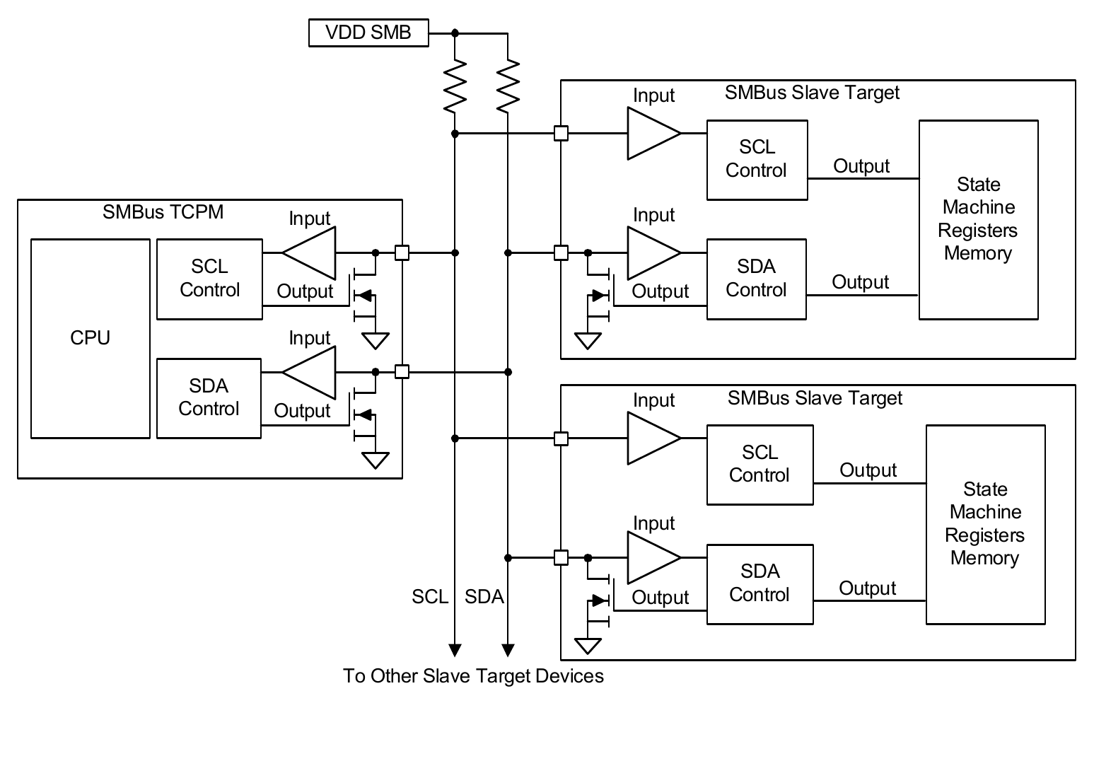
6. General SMBus/I²C Architecture
6.1 Data Validity
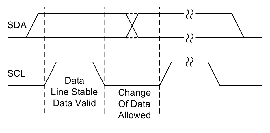
The data on the SDA line must be stable during the HIGH period of the SCL unless generating a START or STOP condition. The HIGH or LOW state of the data line can change only when the clock signal on the SCL line is LOW. See Figure 15.
6.2 START and STOP Conditions
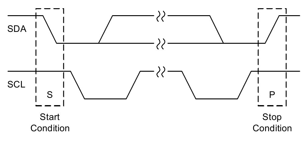
Figure 16 shows that the START condition is a HIGH to LOW transition of the SDA line while SCL is HIGH.
The STOP condition is a LOW to HIGH transition on the SDA line while SCL is HIGH. A STOP condition must be sent before each START condition.
6.3 Acknowledge (ACK)
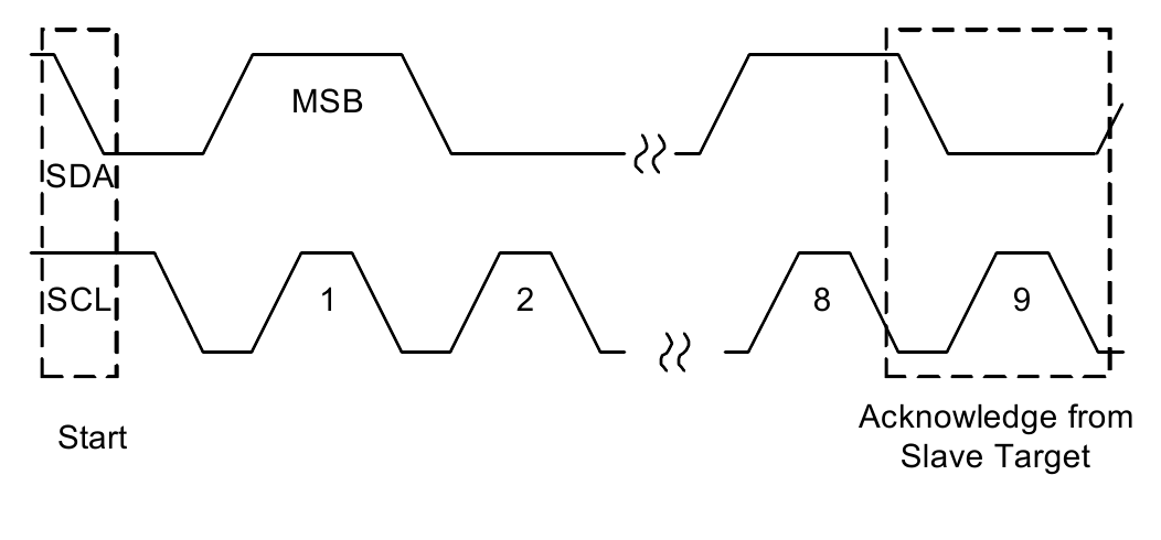
Each address and data transmission uses nine clock pulses. The ninth pulse is the Acknowledge bit (ACK). After the start condition, the TCPM sends seven slave target address bits and a R/W bit during the next eight clock pulses. During the ninth clock pulse, the device that recognizes its own address holds the data line LOW to acknowledge (see Figure 17). Both the TCPM and slave target use the ACK bit to acknowledge receipt of register addresses and data.
6.4 Writing Single Byte Registers
When writing to a single byte register, use the following transaction.
S | Slave Address | Wr(0) | A(0) | Register Address | A(0) | Write Data | A(0) | P
| # | Field | Value |
|---|---|---|
| 1 | S |
START |
| 2 | Slave Address | 7-bit |
| 3 | Wr |
(0) |
| 4 | A |
(0) |
| 5 | Register Address | 8-bit |
| 6 | A |
(0) |
| 7 | Write Data | 8-bit |
| 8 | A |
(0) |
| 9 | P |
STOP |

6.5 Reading Single Byte Registers
When reading to a single byte register, use the following transaction.
S  | Slave Address | Wr(0) | A(0) | Register Address | A(0) | ...
Sr | Slave Address | Rd(1) | A(0) | Read Data | N(1) | P
| # | Field | Value |
|---|---|---|
| 1 | S |
START |
| 2 | Slave Address | 7-bit |
| 3 | Wr |
(0) |
| 4 | A |
(0) |
| 5 | Register Address | 8-bit |
| 6 | A |
(0) |
| 7 | Sr |
Repeated START |
| 8 | Slave Address | 7-bit |
| 9 | Rd |
(1) |
| 10 | A |
(0) |
| 11 | Read Data | 8-bit (shaded = data returned by the target) |
| 12 | N |
(1) NACK |
| 13 | P |
STOP |

6.6 Writing Two-Byte Registers
When writing to a two-byte register, use the following transaction.
S | Slave Address | Wr(0) | A(0) | Register Address | A(0) | Write Data (Low) | A(0) | Write Data (High) | A(0) | P
| # | Field | Value |
|---|---|---|
| 1 | S |
START |
| 2 | Slave Address | 7-bit |
| 3 | Wr |
(0) |
| 4 | A |
(0) |
| 5 | Register Address | 8-bit |
| 6 | A |
(0) |
| 7 | Write Data (Low) | 8-bit |
| 8 | A |
(0) |
| 9 | Write Data (High) | 8-bit |
| 10 | A |
(0) |
| 11 | P |
STOP |

6.7 Reading Two-Byte Registers
When reading a two-byte register, use the following transaction.
S  | Slave Address | Wr(0) | A(0) | Register Address | A(0) | ...
Sr | Slave Address | Rd(1) | A(0) | Read Data (Low) | A(0) | Read Data (High) | N(1) | P
| # | Field | Value |
|---|---|---|
| 1 | S |
START |
| 2 | Slave Address | 7-bit |
| 3 | Wr |
(0) |
| 4 | A |
(0) |
| 5 | Register Address | 8-bit |
| 6 | A |
(0) |
| 7 | Sr |
Repeated START |
| 8 | Slave Address | 7-bit |
| 9 | Rd |
(1) |
| 10 | A |
(0) |
| 11 | Read Data (Low) | 8-bit (shaded) |
| 12 | A |
(0) |
| 13 | Read Data (High) | 8-bit (shaded) |
| 14 | N |
(1) NACK |
| 15 | P |
STOP |

6.8 Writing the TRANSMIT_BUFFER
When writing to the TRANSMIT_BUFFER register, use the following transaction.
S | Slave Address | Wr(0) | A(0) | Register Address (TRANSMIT_BUFFER) | A(0) | ...
  | Write Data (I2C_WRITE_BYTE_COUNT = M + 1) | A(0)
  | Write Data (TX_BUF_BYTE_0) | A(0) | ...
  | Write Data (TX_BUF_BYTE_M) | A(0) | P
| # | Field | Value |
|---|---|---|
| 1 | S |
START |
| 2 | Slave Address | 7-bit |
| 3 | Wr |
(0) |
| 4 | A |
(0) |
| 5 | Register Address (TRANSMIT_BUFFER) |
8-bit |
| 6 | A |
(0) |
| 7 | Write Data (I2C_WRITE_BYTE_COUNT = M + 1) |
8-bit |
| 8 | A |
(0) |
| 9 | Write Data (TX_BUF_BYTE_0) |
8-bit |
| 10 | A |
(0) |
| 11 | ・・・ |
Additional TX_BUF_BYTE_n / A (0) pairs |
| 12 | Write Data (TX_BUF_BYTE_M) |
8-bit |
| 13 | A |
(0) |
| 14 | P |
STOP |

6.9 Reading the RECEIVE_BUFFER
When reading the RECEIVE_BUFFER register, use the following transaction.
S  | Slave Address | Wr(0) | A(0) | Register Address (RECEIVE_BUFFER) | A(0) | ...
Sr | Slave Address | Rd(1) | A(0)
   | Read Data (READABLE_BYTE_COUNT = M + 2) | A(0)
   | Read Data (RX_BUF_FRAME_TYPE) | A(0) | ...
   | Read Data (RX_BUF_BYTE_0) | A(0) | ...
   | Read Data (RX_BUF_BYTE_M) | N(1) | P
| # | Field | Value |
|---|---|---|
| 1 | S |
START |
| 2 | Slave Address | 7-bit |
| 3 | Wr |
(0) |
| 4 | A |
(0) |
| 5 | Register Address (RECEIVE_BUFFER) |
8-bit |
| 6 | A |
(0) |
| 7 | Sr |
Repeated START |
| 8 | Slave Address | 7-bit |
| 9 | Rd |
(1) |
| 10 | A |
(0) |
| 11 | Read Data (READABLE_BYTE_COUNT = M + 2) |
8-bit (shaded) |
| 12 | A |
(0) |
| 13 | Read Data (RX_BUF_FRAME_TYPE) |
8-bit (shaded) |
| 14 | A |
(0) |
| 15 | Read Data (RX_BUF_BYTE_0) |
8-bit (shaded) |
| 16 | A |
(0) |
| 17 | ・・・ |
Additional RX_BUF_BYTE_n / A (0) pairs |
| 18 | Read Data (RX_BUF_BYTE_M) |
8-bit (shaded) |
| 19 | N |
(1) NACK |
| 20 | P |
STOP |

6.10 Reading the Alert Response Address
When reading the Alert Response Address register, use the following transaction.
S | Alert Response Address (0x0C) | Rd(1) | A(0) | Address | Wr(0) | N(1) | P
| # | Field | Value |
|---|---|---|
| 1 | S |
START |
| 2 | Alert Response Address | 0x0C |
| 3 | Rd |
(1) |
| 4 | A |
(0) |
| 5 | Address | 7-bit (shaded = returned by the target) |
| 6 | Wr |
(0) |
| 7 | N |
(1) NACK |
| 8 | P |
STOP |
