A. ECAD Design Information
This information supports the development of the PCB ECAD model for this device. It is intended to be used by PCB designers.
A.1 Part Number Indexing
| Orderable Part Number |
Number of Pins |
Package Type |
Package Code/POD Number |
| RAA489118ARGNP#AA0 |
32 |
TQFN |
L32.4x4D |
| RAA489118ARGNP#HA0 |
32 |
TQFN |
L32.4x4D |
| RAA489118A3GNP#AA0 |
32 |
TQFN |
L32.4x4D |
| RAA489118A3GNP#HA0 |
32 |
TQFN |
L32.4x4D |
| RAA489118A3GNP#MA0 |
32 |
TQFN |
L32.4x4D |
A.2 Symbol Pin Information
A.2.1 32-TQFN
| Pin Number |
Primary Pin Name |
Primary Electrical Type |
Alternate Pin Name(s) |
| 1 |
CSON |
Input |
- |
| 2 |
CSOP |
Input |
- |
| 3 |
VSYS |
Input |
- |
| 4 |
BOOT2 |
Power |
- |
| 5 |
UGATE2 |
Output |
- |
| 6 |
PHASE2 |
Power |
- |
| 7 |
LGATE2 |
Output |
- |
| 8 |
VDDP |
Power |
- |
| 9 |
LGATE1 |
Output |
- |
| 10 |
PHASE1 |
Power |
- |
| 11 |
UGATE1 |
Output |
- |
| 12 |
BOOT1 |
Power |
- |
| 13 |
ASGATE |
Output |
- |
| 14 |
CSIN |
Input |
- |
| 15 |
CSIP |
Input |
- |
| 16 |
ADP |
Input |
- |
| 17 |
DCIN |
Power |
- |
| 18 |
VDD |
Power |
- |
| 19 |
ACIN |
Input |
- |
| 20 |
OTGEN |
Input |
CMIN |
| 21 |
SDA |
I/O |
- |
| 22 |
SCL |
I/O |
- |
| 23 |
PROCHOT# |
Output |
- |
| 24 |
ACOK |
Output |
- |
| 25 |
BATGONE |
Input |
- |
| 26 |
OTGPG |
Output |
CMOUT |
| 27 |
PROG |
Input |
- |
| 28 |
COMP |
Output |
- |
| 29 |
AMON |
Output |
BMON |
| 30 |
CONFIG |
I/O |
PSYS |
| 31 |
VBAT |
Input |
- |
| Pin Number |
Primary Pin Name |
Primary Electrical Type |
Alternate Pin Name(s) |
| 32 |
BGATE |
Output |
- |
| EPAD33 |
GND |
Power |
- |
A.3 Symbol Parameters
| Orderable Part Number |
Qualification |
Mounting Type |
Min Input Voltage |
Max Input Voltage |
Min Output Voltage |
Max Output Voltage |
Min Operating Temperature |
Max Operating Temperature |
RoHS |
Trickle Charging |
Typ Switching Frequency |
Switcher Configuration |
| RAA489118ARGNP#AA0 |
Consumer |
SMD |
3.9 V |
30 V |
2.4 V |
30.8 V |
-10° C |
+100° C |
Yes |
Yes |
732 KHz |
Buck, Boost, and Buck-Boost |
| RAA489118ARGNP#HA0 |
Consumer |
SMD |
3.9 V |
30 V |
2.4 V |
30.8 V |
-10° C |
+100° C |
Yes |
Yes |
732 KHz |
Buck, Boost, and Buck-Boost |
| RAA489118A3GNP#AA0 |
Industrial |
SMD |
3.9 V |
30 V |
2.4 V |
30.8 V |
-40° C |
+105° C |
Yes |
Yes |
732 KHz |
Buck, Boost, and Buck-Boost |
| RAA489118A3GNP#HA0 |
Industrial |
SMD |
3.9 V |
30 V |
2.4 V |
30.8 V |
-40° C |
+105° C |
Yes |
Yes |
732 KHz |
Buck, Boost, and Buck-Boost |
| RAA489118A3GNP#MA0 |
Industrial |
SMD |
3.9 V |
30 V |
2.4 V |
30.8 V |
-40° C |
+105° C |
Yes |
Yes |
732 KHz |
Buck, Boost, and Buck-Boost |
A.4.1 32-TQFN
| IPC Footprint Type |
Package Code/ POD number |
Number of Pins |
| QFN |
L32.4x4D |
32 |
| Description |
Dimension |
Value (mm) |
Diagram |
| Minimum body span (vertical side) |
Dmin |
3.95 |
|
| Maximum body span (vertical side) |
Dmax |
4.05 |
|
| Minimum body span (horizontal side) |
Emin |
3.95 |
|
| Maximum body span (horizontal side) |
Emax |
4.05 |
|
| Minimum Lead Width |
Bmin |
0.15 |
|
| Maximum Lead Width |
Bmax |
0.25 |
|
| Minimum Lead Length |
Lmin |
0.25 |
|
| Maximum Lead Length |
Lmax |
0.35 |
|
| Maximum Height |
Amax |
0.8 |
|
| Minimum Standoff Height |
A1min |
0 |
|
| Minimum Lead Thickness |
cmin |
0.15 |
|
| Maximum Lead Thickness |
cmax |
0.25 |
|
| Number of pins (vertical side) |
PinCountD |
8 |
|
| Number of pins (horizontal side) |
PinCountE |
8 |
|
| Distance between the center of any two adjacent pins (vertical side) |
PitchD |
0.4 |
|
| Distance between the center of any two adjacent pins (horizontal side) |
PitchE |
0.4 |
|
| Location of pin 1; S2 = corner of D side, C1 = center of E side |
Pin1 |
S2 |
|
| Minimum thermal pad size (vertical side) |
D2min |
2.6 |
|
| Maximum thermal pad size (vertical side) |
D2max |
2.8 |
|
| Minimum thermal pad size (horizontal side) |
E2min |
2.6 |
|
| Maximum thermal pad size (horizontal side) |
E2max |
2.8 |
|
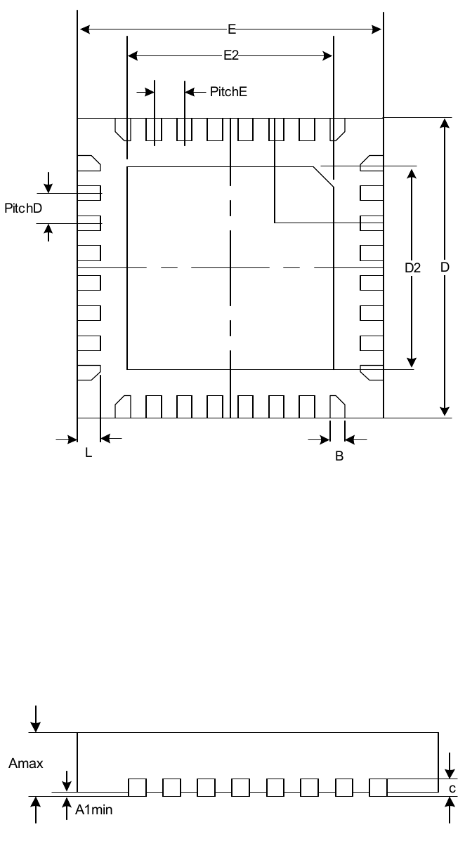
The "Diagram" column of the table above is a single cell spanning every row. It
holds the following drawings, which carry no printed figure number and no
printed caption:
| Recommended Land Pattern |
Recommended Land Pattern |
Recommended Land Pattern |
Recommended Land Pattern |
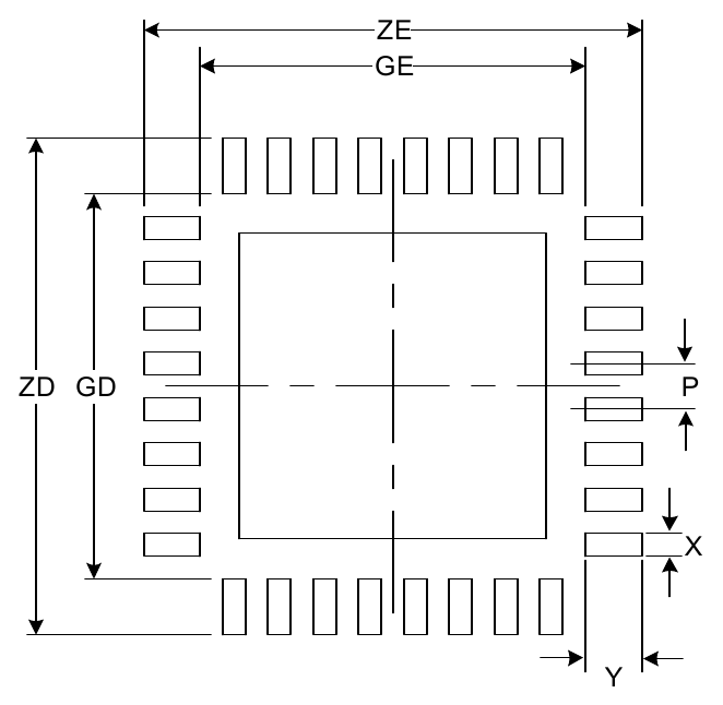
| Description |
Dimension |
Value (mm) |
Diagram |
| Distance between left pad toe to right pad toe (horizontal side) |
ZE |
4.4 |
|
| Distance between top pad toe to bottom pad toe (vertical side) |
ZD |
4.4 |
|
| Distance between left pad heel to right pad heel (horizontal side) |
GE |
3.4 |
|
| Distance between top pad heel to bottom pad heel (vertical side) |
GD |
3.4 |
|
| Pad Width |
X |
0.2 |
|
| Pad Length |
Y |
0.5 |
|
The "Diagram" column of the Recommended Land Pattern table is a single cell
spanning every row. It holds the following drawing, which carries no printed
figure number and no printed caption: